Download
1 / 6
60 likes | 154 Views
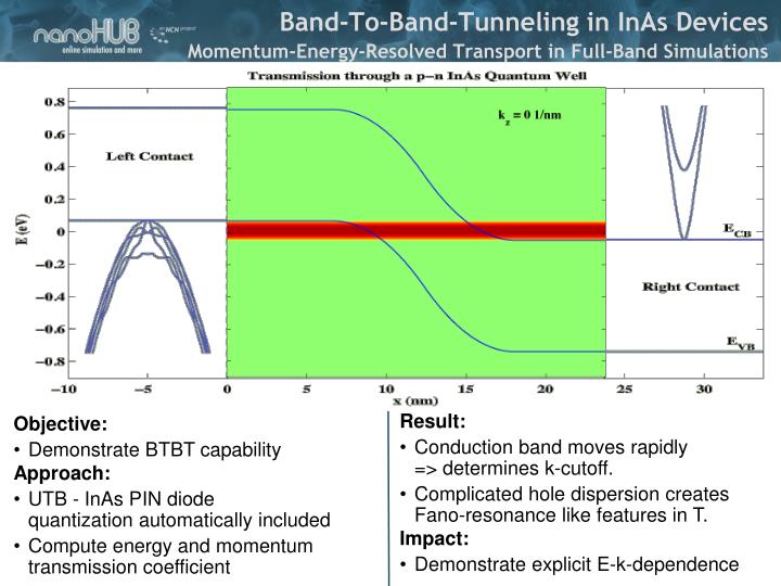
Band-To-Band-Tunneling in InAs Devices Momentum-Energy-Resolved Transport in Full-Band Simulations. Result: Conduction band moves rapidly => determines k-cutoff. Complicated hole dispersion creates Fano-resonance like features in T. Impact: Demonstrate explicit E-k-dependence. Objective:

E N D
Band-To-Band-Tunneling in InAs Devices Momentum-Energy-Resolved Transport in Full-Band Simulations • Result: • Conduction band moves rapidly=> determines k-cutoff. • Complicated hole dispersion creates Fano-resonance like features in T. • Impact: • Demonstrate explicit E-k-dependence • Objective: • Demonstrate BTBT capability • Approach: • UTB - InAs PIN diodequantization automatically included • Compute energy and momentum transmission coefficient
Band-To-Band-Tunneling in InAs Devices Charge Self-consistent Full-Band Transport in Realistic Structure Bandgap raised from bulk 0.37=>0.6eV Doping 1x10¹⁸/cm3 • Impact: • First full band / atomistic charge-self-consistent BTBT simulation • Full ambipolar carrier treatment • Objective: • Demonstrate BTBT capability • Approach: • Full I-V calculation in OMEN
Band-To-Band-Tunneling in InAs Devices Charge Self-consistent Full-Band Transport in Realistic Structure Bandgap raised from bulk 0.37=>0.6eV Doping 1x10¹⁸/cm3 • Impact: • First full band / atomistic charge-self-consistent BTBT simulation • Full ambipolar carrier treatment • Objective: • Demonstrate BTBT capability • Approach: • Full I-V calculation in OMEN
Band-To-Band-Tunneling in InAs Devices Charge Self-consistent Full-Band Transport in Realistic Structure Bandgap raised from bulk 0.37=>0.6eV Doping 1x10¹⁸/cm3 • Impact: • First full band / atomistic charge-self-consistent BTBT simulation • Full ambipolar carrier treatment • Objective: • Demonstrate BTBT capability • Approach: • Full I-V calculation in OMEN
Gate Control and Sub-Threshold Swing in BTBT Comparison of pin InAs pin Devices – SG-UTB / DG-UTB / NW • Objective: • Low voltage, good turn-on/off switches • Develop low sub-threshold swing FETs with band-to-band-tunneling (BTBT) • Provide guidance to experiments • Approach: • Utilized OMEN – atomistic, full band quantum transport simulator • 3 diff. geom., InAs, 20nm gates. 6nm body/diameter, 1nm Oxide, 5e19/cm3 • Result – 3 different devices have: • dramatically different sub-thresholds • Slightly different gate controls • Impact: • BTBTdevices much more sensitive to smooth band bending than expected • gate all-around NW fairs best. • Authors: • M. Luisier, Gerhard Klimeck