Download
1 / 12
180 likes | 533 Views
The Basic Memory Element - The Flip-Flop.

E N D
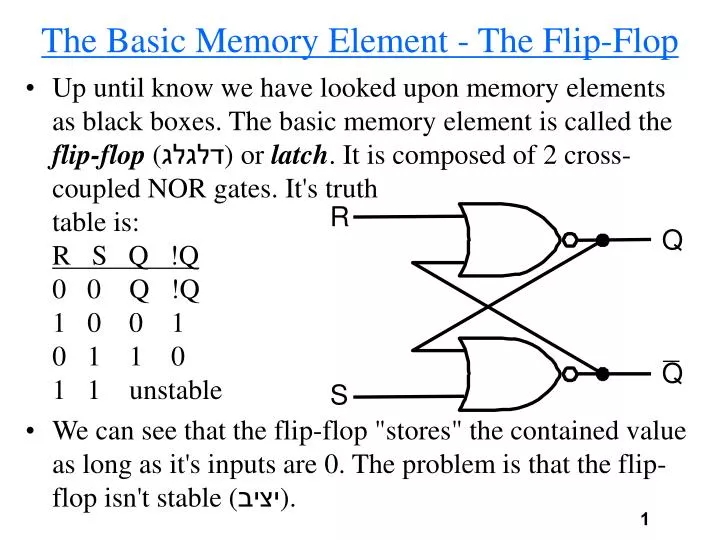
The Basic Memory Element - The Flip-Flop • Up until know we have looked upon memory elements as black boxes. The basic memory element is called the flip-flop (דלגלג) or latch. It is composed of 2 cross-coupled NOR gates. It's truthtable is:R S Q !Q0 0 Q !Q1 0 0 10 1 1 01 1 unstable • We can see that the flip-flop "stores" the contained value as long as it's inputs are 0. The problem is that the flip-flop isn't stable (יציב).
The D Flip-Flop • Adding 2 AND gates to the flip-flop turns it into a stable memory element. The 2 inputs are C (clock) and D (data). When C is asserted (set to 1) the ff is open, the value of D is stored in it, and Q becomes D. When C is deasserted the ff is closed and Q is the value of whatever was stored the last time the ff was open. • This type of flip-flop is activated by the rising edge of the clock. As the clockdiagram shows:
The Master-Slave Flip-Flop • In order to implement a falling clock ff we use 2 D flip-flops called a master-slave flip-flop. Now the value Q changes on the falling edge of the clock.
The Register File • The register-file has to enable us to read1 or 2 registers and write into 1 register. The read part is easy we use 2 MUXs to choose the registers that are read. • For the write part we use a decoder, given a number i it asserts the ith line and deasserts all other lines. This line together with the write signal provide the C input to each register.
SRAM (Static Random Access Memory) • Larger amounts of memory than register-files are built with SRAMs. A SRAM chip is a circuit that stores many memory elements and enables access to one at a time. SRAMs have fixed access time to any memory element. • A 256K x 1 SRAM can hold 256 entries each of which is 1-bit wide. Thus it will have 18 address lines (256K=218), 1 data input line and 1 data output line. A 32K x 8 SRAM has the same amount of total bits but has 15 address lines, 8 input and 8 output lines. The number of possible addresses is called the height and the number of bits in each location is called the width. Typical accesstimes are 5-25 ns.
The Three-State Buffer • To build large memories we would need giant MUXs in order to read their contents (look at the register-file diagram). For a 64K x1 SRAM we would need a 64K to 1 MUX. • Instead large memories are implemented by using a shared output line called a bit-line. To allow multiple source to set a single line we use the three-state buffer (or tri-state buffer). A three-state buffer has 2 inputs: a data-signaland an Output enable. The single output is the data-signal if the Output enable is set (1). If the Output enable is 0 the output of the buffer is in ahigh-impedance state which enables other three-state buffers to set the bit-line. • A 4-way MUX is composed of 4 three-state buffers.
A 32K x 8 SRAM • We still need a large decoder and a large number of word lines (the lines used to enable the individual cells). • The solution is to organize memories as rectangular (מלבני) arrays and use a 2-step decoding process: The 1st decoder creates an address for the eight 512x64 arrays. Then a set of MUXs selects 1 bit out of every 64 bit-wide array.
DRAM (Dynamic Random Access Memory) • In SRAM the value stored in a cell is kept on a pair of inverting gates as long as the power is on. In Dynamic RAM the value kept in a cell is stored as a charge (מטען) in a capacitor (קבל). A single transistor is used to access this value. • Because DRAMs use 1 transistor per bit they are cheaper and denser (צפופים) then SRAM which use 4-6 transistors per bit. • In DRAM the charge must be refreshed by reading it and writing it back again. This is why it is called dynamic RAM. • The charge can be kept for several milliseconds which is close to a million clock cycles. • If we had to refresh each bit we would have no time left to read or write data. • Fortunately DRAMs use a 2-level decoding structure which enables refreshing an entire row at once. Typically, refresh operations take 1-2% of the active cycles of the DRAM.
A 4M x 1 DRAM • DRAMs use a 2-level decoder: a row-access followed by a column-acess. The row-access chooses a row and stores it in a set of column latches. The column-access use a MUX to select the data from the row. To save pins (פינים, רגליים) the same address lines are used for both the row and column addresses: A pair of signals RAS (Row Access Strobe) and CAS (Column Access Strobe) are used to signal if a row or column address is being supplied. • Refresh is performed by reading a row and writing the values back. • In 1997, typical DRAM access times are 60-110ns. The cost perbit makes DRAM ideal for main memory. The speed of SRAMmakes it ideal for caches.
EDO and SDRAMs • A 4M x1 DRAM reads 2048 bits on every row-access and throws away 2047 bits. It is possible to provide higher bandwidth by allowing a column address change without a row address change, resulting in an access to bits in the column latches. This is called page-mode or static-column mode. • Nibble-mode RAMs internally create the next 3 column address thus provding 4 bits (a nibble) for every row access. • EDO (Extended Data Out) RAMS are the latest versions of page-mode style. They are becoming standard and have an access time of 25ns. • SDRAMs(Synchronous DRAMS) and SSRAMs enable reading or writing a burst of data from sequential addresses in a row or in a column. SDRAMs and SSRAMs are used mainly in caches where blocks of data are transferred.
Error Detection and Correction • Because of potential data corruption in large memories. Most computers use some sort of error-checking code. • One simple code that is used is a parity code. The number of 1s in a word is counted. The word has odd parity if the number of 1s is odd and even parity if the number of 1s is even. The parity bit is written into memory along with the word (1 for odd, 0 for even). • When the word is read so is the parity bit, if the parity stored doesn't match the parity read an error is signaled. • A 1 bit parity can detect only 1 bit of error. • Parity is only an error-detection scheme. There are more complex error correction codes (ECC) which can correct errors in several bits.