Download
1 / 16
160 likes | 244 Views
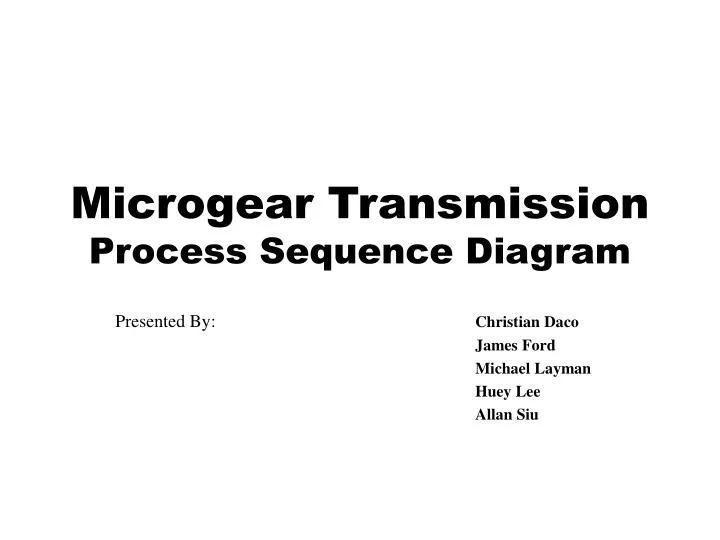
Microgear Transmission Process Sequence Diagram. Presented By: Christian Daco James Ford Michael Layman Huey Lee Allan Siu. Starting with a silicon substrate…. Silicon Substrate. 1. LPCVD 2 m layer silicon dioxide (SiO 2 ).

E N D
Microgear TransmissionProcess Sequence Diagram Presented By: Christian Daco James Ford Michael Layman Huey Lee Allan Siu
Starting with a silicon substrate… Silicon Substrate
1. LPCVD 2 m layer silicon dioxide (SiO2) SiH4 + O2 SiO2 + H2 @ Temp 400 – 500 C Silicon Dioxide Silicon Substrate
2. LPCVD 1m polysilicon layer. SiH4 Si + 2H2 @ Temp = 600-650 C Polysilicon Layer #1 Silicon Dioxide Silicon Substrate
3. Coat photoresist. Photoresist Polysilicon Layer #1 Silicon Dioxide Silicon Substrate
4. Expose and develop photoresist. Photoresist Polysilicon Layer #1 Silicon Dioxide Silicon Substrate
5. Etch polysilicon layer by plasma etching in Cl2 to expose silicon dioxide layer. Photoresist Polysilicon Layer #1 Silicon Dioxide Silicon Substrate
6. Strip photoresist in H2SO4/H2O2 Polysilicon Layer #1 Silicon Dioxide Silicon Substrate
7. Wet etch SiO2 layer with HF Polysilicon Layer #1 Silicon Dioxide Silicon Substrate
8. Deposit sacrificial SiO2 layer conformally with tetraethylorthosilicate (TEOS) Silicon Dioxide Polysilicon Layer #1 Silicon Dioxide Silicon Substrate
9. Deposit 1m polysilicon layer with LPCVD. Polysilicon Layer #2 Silicon Dioxide Polysilicon Layer #1 Silicon Dioxide Silicon Substrate
10. Apply photoresist and pattern gear shape. Photoresist Polysilicon Layer #2 Silicon Dioxide Polysilicon Layer #1 Silicon Dioxide Silicon Substrate
(Zoom out view to see gear formation) Photoresist Polysilicon Layer #2 Silicon Dioxide Polysilicon Layer #1 Silicon Dioxide Silicon Substrate
11. Plasma dry etch in Cl2 to create gear shape Photoresist Polysilicon Layer #2 Silicon Dioxide Polysilicon Layer #1 Silicon Dioxide Silicon Substrate
(Zoom in) 12. Strip photoresist in H2SO4/H2O2 Polysilicon Layer #2 Silicon Dioxide Polysilicon Layer #1 Silicon Dioxide Silicon Substrate
13. Wet etch SiO2 layer with HF to release gear. Polysilicon Layer #2 Silicon Dioxide Polysilicon Layer #1 Silicon Dioxide Silicon Substrate Silicon Substrate