Download
1 / 62
880 likes | 1.45k Views
Chapter 6 Registers and Counters. 6-1 Registers. 6-2 Shift Registers. 6-3 Ripple Counters. 6-4 Synchronous Counters. 6-5 Other Counters. 6-6 HDL for Registers and Counters. 6-1 Registers.

E N D
Chapter 6 Registers and Counters 6-1 Registers 6-2 Shift Registers 6-3 Ripple Counters 6-4 Synchronous Counters 6-5 Other Counters 6-6 HDL for Registers and Counters
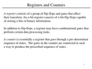
6-1 Registers A collection of two or more D flip-flops with a common clock input is called a register. In its broadest definition, a register consists of a group of flip-flops and gates that effect their transition. A simplest register constructed with 4 D flip-flops
6-1 Registers Two basic functions of a register : data storage and data movement. The shifting capability of a register permits the movement of data from stage to stage within the register or into or out of the register upon application of clock pulse. The storage capability of a register makes it an important type of memory device.
6-1 Registers When the clear input goes to 0, flip-flops are reset asynchronously. The common clock inputs triggers all flip-flops on the positive edge of each pulse and the binary data available at the four inputs are transferred into the 4-bit register.
6-1 Registers In this configuration, the clock must be inhibited from the circuit if the content of the register must be left unchanged. However, inserting enabling gates to do that produces uneven propagation delays between the clock and the inputs of flip-flops.
6-1 Registers It is advisable to control the operation of the register with the D inputs rather than controlling the clock in the C inputs of the flip-flops. The load input to register determines the action to be taken with each clock pulse.
6-2 Shift Registers A register capable of shifting its binary information in one or both directions is called a shift register. Shift registers consist of an arrangement of flip-flops in cascade.
6-2 Shift Registers The serial transfer of information from register A to register B • Serial Transfer A digital system is said to operate in a serial mode when information is transferred and manipulated one bit at a time.
6-2 Shift Registers Data Serial In • Serial In/Serial Out Shift Register one bit at a time on a single line. It produces the stored information on its output also in serial form. Data Serial Out
6-2 Shift Registers • Serial In/Parallel Out Shift Register Data bits are entered serially into this type of register in the same manner as discussed before. Once the data are stored, each bit appears on its respective output line, and all bits are available simultaneously, rather than on a bit-by-bit basis as with the serial output.
For a register with parallel data inputs, the bits are entered simultaneously into their respective stage on parallel lines rather than on a bit-by-bit basis on one line as with serial data inputs. The serial output is the same as described before. 6-2 Shift Registers • Parallel In/Serial Out Shift Register
6-2 Shift Registers Immediately following the simultaneous entry of all data bits, the bits appear on the parallel outputs • Parallel In/ Parallel Out Shift Register
6-2 Shift Registers • Universal Shift Register Function table for the 4-bit universal shift register If the register can shift in both directions and has parallel load capabilities, it is referred to as a universal shift register.
It consists of four D flip-flops and four multiplexers. The four multiplexers have two common selection inputs s0 and s1.
6-2 Shift Registers Example: 74x194 4-bit universal shift register Function table for the 74x194 4-bit universal shift register. The 74x194 is an MSI 4-bit bidirectional parallel-in, parallel-out shift register.
It consists of: • four D flip-flops • four multiplexers. • The four multiplexers have two common selection inputs s0 and s1.
6-2 Shift Registers The clock signal provides the timing reference for transfers, defining the time to transfer one bit. A synchronization pulse (or sync pulse) provides a reference point for defining the data format, such as the beginning of a byte or word in the serial data stream. • Serial/Parallel Conversion A typical application of serial data transfer between two modules is shown in the following figure. Serial data itself is transmitted on a single line.
Parallel-to- Serial Conversion using a parallel-in shift register Two 74x163 counters are wired as a free-running modulo-256 counter to define the frame.
Parallel-to- Serial Conversion using a parallel-in shift register The five high order and three low-order counter bits are the timeslot number and bit number, respectively.
Parallel-to- Serial Conversion using a parallel-in shift register A 74x166 parallel-in shift register performs the parallel-to-serial conversion.
Serial -to- Parallel Conversion using a parallel-out shift register A modulo-256 counter built from a pair of 74x163s is used to reconstruct the timeslot and bit numbers.
Serial -to- Parallel Conversion using a parallel-out shift register SYNC loads the destination module’s counter with 0 so that both counters go to 0 on the same clock edge.
The counter’s high-order bits (timeslot number) are not used in the figure, but they may be used by other circuits in the destination module to identify the byte from a particular timeslot on the parallel data bus (PD0–PD7).
6-3 Ripple Counters A register that goes through a prescribed sequence of states upon the application of input pulses is called a counter. General structure of a counter’s state diagram —a single cycle The modulus of a counter is the number of states in the cycle.
6-3 Ripple Counters Categories: • synchronous • asynchronous The asynchronous counter is commonly called ripple counter because the carry information ripples from the less significant bits to the more significant bits, one bit at a time. • count-up • count-down • Binary Counter • BCD Counter
4-Bit Binary Ripple Counter with T flip-flop 4-Bit Binary Ripple Counter with D flip-flop 6-3 Ripple Counters • Binary Ripple Counter The output of each flip-flop is connected to the C input of the next flip-flop in sequence. The flip-flop holding the least significant bit receives the incoming count pulse.
0 0 0 0 1 1 1 1 1 1 1 0 0 0 6-3 Ripple Counters • Binary Ripple Counter The least significant bit is complemented with each count pulse input. Every time a bit goes from 1 to 0, it complements the next higher order bit.
6-3 Ripple Counters • Binary Ripple Count-Down Counter The diagram of a binary count-down counter looks same as the right figure, provided all flip-flops trigger on the positive edge of the clock.
6-3 Ripple Counters • BCD Ripple Counter State diagram of a BCD counter
0 0 1 1 1 0 Q1 changes state after each clock pulse. Q2 complements every time Q1 goes from 1 to 0 as long as Q8 =0. when Q8 =1, Q2 remain at 0. 6-3 Ripple Counters • BCD Ripple Counter 0
0 1 1 0 Q4 complements every time Q2 goes from 1 to 0. Q8 remains at 0 as long as Q2 or Q4 is 0. when both Q2 and Q4 become 1, Q8 complements when Q1 goes from 1 to 0. 6-3 Ripple Counters • BCD Ripple Counter
6-4 Synchronous Counters Although a ripple counter requires fewer components than any other type of binary counter, it does so at a price—it is slower than any other type of binary counter. In the worst case, when the most significant bit must change, the output is not valid until time n×tTQ after the rising edge of CLK, where tTQ is the propagation delay from input to output of a T flip-flop. A synchronous counter connects all of its flip-flop clock inputs to the same common CLK signal, so that all of the flip-flop outputs change at the same time, after only tTQ ns of delay.
6-4 Synchronous Counters A synchronous 4-bit binary counter with serial enable logic • Binary Counter Each T flip-flop toggles if and only if CNTEN is asserted and all of the lower-order counter bits are 1.
6-4 Synchronous Counters • Binary Counter the combinational enable signals propagate serially from the least significant to the most significant bits. If the clock period is too short, there may not be enough time for a change in the counter’s LSB to propagate to the MSB.
6-4 Synchronous Counters • Binary Counter How to eliminate the problem? driving each EN input with a dedicated AND gate.
6-4 Synchronous Counters Function Table • Up-Down Binary Counter Inputs to the AND gate from the complement output
6-4 Synchronous Counters • Binary Counter with Parallel Load
6-4 Synchronous Counters • Binary Counter with Parallel Load
0 1 1 0 6-4 Synchronous Counters • BCD Counter State Table N QD QC QB QA 0 0 1 1 0 1 0 1 1 1 2 1 0 0 0 3 1 0 0 1 4 1 0 1 0 5 1 0 1 1 6 1 1 0 0 7 1 1 0 1 8 1 1 1 0 9 1 1 1 1 0 1 1 0 QCC=1
0 0 0 0 6-4 Synchronous Counters • Another Example of BCD Counters State Table N QD QC QB QA 0 0 0 0 0 1 0 0 0 1 2 0 0 1 0 3 0 0 1 1 4 0 1 0 0 5 0 1 0 1 6 0 1 1 0 7 0 1 1 1 8 1 0 0 0 9 1 0 0 1 0 1 0 0 1 0 0 0 0
6-5 Other Counters State Table for Counter • Counter with Unused States Example: realize the following state table
JA = BKA = B JB= C KB =1 JC = B' KC = 1 6-5 Other Counters • Counter with Unused States The simplified equations are: The counter is self-correcting.
6-5 Other Counters State diagram for a ring counter • Ring Counter There are five invalid counting cycle. A circular shift register with only one flip-flop being set at any particular time, all others are cleared.
6-5 Other Counters State diagram for a self-correcting ring counter • Ring Counter
6-5 Other Counters • Ring Counter Self-correcting 4-bit, 4-state ring counter with a single circulating 1
6-5 Other Counters States of a 4-bit Johnson counter. • Johnson Counter An n-bit shift register with the complement of the serial output fed back into the serial input is a counter with 2n states and is called a twisted-ring, Moebius, or Johnson counter.
This circuit loads 0001 as the next state whenever the current state is 0xx0. 6-5 Other Counters • Johnson Counter Self-correcting four-bit, eight-state Johnson counter.
6-6 HDL for Register and Counters • Shift Register
6-6 HDL for Register and Counters Behavioral description of Universal shift register • Shift Register module shftreg (s1,s0,Pin,lfin,rtin,A,CLK,Clr); input s1,s0; //Select inputs input lfin, rtin; //Serial inputs input CLK,Clr; //Clock and Clear input [3:0] Pin; //Parallel input output [3:0] A; //Register output reg [3:0] A; always @ (posedge CLK ornegedge Clr) if (~Clr) A = 4'b0000; else case ({s1,s0}) 2'b00: A = A; //No change 2'b01: A = {rtin,A[3:1]}; //Shift right 2'b10: A = {A[2:0],lfin}; //Shift left 2'b11: A = Pin; //Parallel load input endcase endmodule The always block describes the five operations that can be performed with the register.