Download
1 / 18
180 likes | 281 Views
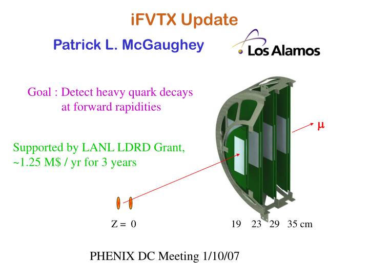
iFVTX Update. Patrick L. McGaughey. Goal : Detect heavy quark decays at forward rapidities. m. Supported by LANL LDRD Grant, ~1.25 M$ / yr for 3 years. Z = 0 19 23 29 35 cm. PHENIX DC Meeting 1/10/07. Pixel-based iFVTX.

E N D
iFVTX Update Patrick L. McGaughey Goal : Detect heavy quark decays at forward rapidities m Supported by LANL LDRD Grant, ~1.25 M$ / yr for 3 years Z = 0 19 23 29 35 cm PHENIX DC Meeting 1/10/07
Pixel-based iFVTX • LANL/ FNAL/ Columbia / UNM/ NMSU / ISU collaboration • Designed to measure distance of closest approach of tracks to the primary vertex • 4 planes of pixel tiles with FPIX chip (BTeV) bump bonded to a Silicon sensor • Provides a DCA resolution of sDCA ~ 100-200 microns • Can send data to prototype Lvl-1 trigger boards Measures : D (charm) μ + X B (beauty) μ + X 8 chip plane Silicon Sensor
m iFVTX Detector Planes 24 ea 8 chip modules 12 ea on front/back 15 cm 7 cm Z = 0 19 23 29 35 cm • 4 Tracking stations composed of Si pixels, 50 by 400 um • Cover ~ 1/8 of one muon arm (one octant) with ~100 detector modules • Electronics recently developed by FNAL for BTeV, ~2M pixels. • Low power, high speed and high resolution pixel detector. • Can detect large numbers ofD and some B decays per year at RHIC.
Dramatic Signal / Background Improvement for Heavy Quarks After vertex cuts Before vertex cuts Muon Events charm Background charm Background beauty pT (GeV/c) pT (GeV/c) Simulated Signal to Noise for D +X without and with vertex cuts, 10 X improvement in signal / background accurateyield, slope of charm
Heavy Quark Yields*, for 1/8 of a Muon Arm • Rates before application of a • vertex cut. Z-Vertex Resolution, m Muon Momentum, GeV
iFVTX Status - Detector Elements • Silicon Pixel Detectors • Total 28 wafers (6 detectors per wafer) fabricated by CIS, tested at CIS and UNM. More than enough for iFTX + spares • Excellent yields (~93%), only 1 bad wafer from 1st 20. • Front End Chip (FPIX2) • Total 11 wafers produced by MOSIS / TSMC. • 1 wafer tested, good yield (~77%). Should have plenty of good die. Testing underway. • Flip Chip Assembly of Detector Modules (Bump Bonding) • ~30 prototype multi-chip modules delivered from VTT. • Testing underway, yield low due to use of untested FPIX chips. • Will submit pre-production parts to VTT soon. • High Density Interconnect (Kapton bus) • Prototypes delivered from CERN are OK, but yield was poor. • Have re-designed a simpler HDI, first deliveries mid Jan.
iFVTX Status - Mechanical • Picture Frame (Detector Plane PC Board) • Prototype being designed at FNAL, uses TPG to transfer heat to liquid cooling. • Thermal issues have been studied, appropriate glues selected • Mechanical Support Structure • Design underway at HYTEC. • Will fit into same cage design as FVTX and not interfere with VTX. • Cooling System • Haven’t chosen coolant temperature yet, may want detector to operate at room temperature. • Heat load should not be a problem (FPIX < 200 W). • FPIX / Sensor Modules • Plan to assemble and test at FNAL.
iFVTX Status - DAQ • Pixel Module Test Stand • FPGA/PCI readout card and software are working. • Calibration and monitoring • Pulse injection system prototyped and working. • Current, voltage and temperature monitor working. • Columbia/Nevis DAQ approach : • FPGA at detector receives data driven FPIX output, sends to counting house over fiber. • Receiver on PCI card in PHENIX DAQ farm uses DMA to put selected data into event memory. • Prototype system tested and working with standalone PC. • LANL approach : ROC, FEM and DCM • Read Out Controller has FPGA at detector, sends data to : • Front End Module selects triggered event data, sends data to standard PHENIX DCM. • ROC and FEM prototypes working with interface to PC, no fiber interface yet.
LANL FPIX2.1 / sensor Calibration Results • Realistic triggered readout. • Results of threshold scan reproduce FNAL test results. • The proposed readout design is working as expected • 7 min required for 100 pulses at 64 amplitude settings. • One pixel tested at a time, Measured noise is 140 electrons!
Hardware Completion Schedule • FY06 : HDI designed done First pixel modules flip chip assembled done Si sensors delivered done FPIX2.1 readout chips delivered done Test bench DAQ systems done • FY07 : Decision on DAQ design 03/07 HDI Production 05/07 Flip chip Si detectors and FPIX readout chips 08/07 Beam test of a few modules ??? • FY08 : Pixel plane printed circuit boards 10/07 Pixel module assembly 03/08 DAQ Electronics 03/08 Pixel plane assembly 06/08 • FY09 : Full system testing outside of PHENIX 12/08 Ready for installation in PHENIX, needs VTX for primary vertex determination. Useful with p-p, d-Au or Au-Au beams
Benefits to FVTX Program • Expect to use same readout design and test stands for iFVTX and FVTX. • Share same mechanical support structure with FVTX, with one additional insert for iFVTX. Can be assembled independently of VTX, FVTX. • Simulation and analysis tools developed for iFVTX work for FVTX as well. Mainly a change in the length of the pixels. • Experience gained with hit rates, noise levels, etc will provide useful input for FVTX program. • Several man-years of R+D work are being paid by our LDRD grant, much of which is of direct value to the FVTX.
Next Steps with PHENIX ? • Letter of intent. • Timing of installation with respect to HBD, VTX, FVTX. • Required PHENIX DAQ resources and systems integration. • What else ?
Multichip module BTeV Pixel Detector Module Si pixel sensors FPIX 2 Pixel Readout chip • Pixel Sensor bump-bonded to Readout chip • Fine segmentation • 50 mm x 400 mm • Large number of channels • Electronics in the active tracking volume • High power density cooling system required • Basic building block – Multichip Module (MCM) • 8 readout chips / module • HDI and flex cables • Assemble modules on both sides of substrate to form pixel plane; providing a high resolution radius measurement plus a good phi measurement. 50 um 400 um Module Assembly
Nevis FPIX Interface Optical Transceiver Inject Pulser Logic FPIX 6-bit Pulser Shift Out Command Interpreter Serdes Shift In • Current design reads single FPIX with 1- or 4-lines • Altera Cyclone FPGA • No provision for time-ordering pixel data • Includes 15-bit counter to implement timed commands and timestamps • FIFO buffers non-immediate commands (128 deep) FIFO Shift Control Data Lines Packet Logic Phase Follower Logic Deserializer BCO 80 MHz Clock Data Clk VDDD Regulated power VDDA
Nevis FPIX Receiver Routing and Tx Logic Memory Serdes Optical Tx/Rx • Implemented as 32-bit 33 MHz PCI card • Provides 3 channels: Control out, control in, data in • Communicates with user via registers • Dataflow governed by ABC register architecture (one set of ABC per channel) • A : physical RAM address (in PC) of next DMA transfer • B : physical RAM address (in PC) of next user access • C: contains bookkeeping to allow pci card to know when/where to wrap A values • Uses ACEX family FPGA • 256 kB SRAM on-board PCI Register Logic 80MHz clock DMA Tx 33 MHz 32-bit PCI Bus
Near Silicon Outside IR To Level 1 trigger • Serial download to chips • Pass beam clock • Initialize/Reset Arcnet (FPGA program., chip download) T+FC Data compressor, Serializer, Optical Driver DCM Data Buffer, FPGA 2.5 Gb/s FPIX2.1 • 1,2,4,(6) lines/chip • Stream of 24-bit data words with: • Location • (3 bit ADC) • Beam Clock Counter • 140Mbps readout lines can drive 10 m Uses commercial driver • Buffers Data • Upon lvl1 grab relevant data • Build packet • DataDCM • Pass beam clock • Initialize chips PHENIX Standard LANL Pixel Detector Readout Design • Readout electronics split into two parts • Near the detector • Compresses and serializes the data from a group of chips • Radiation tolerance use FLASH based FPGAs from Actel • Fiber link to the control room • In the Control Room (FEM) • Buffer data for 64 beam clocks • Write data upon LVL1 trigger request • SRAM based FPGAs from Xilinx (Altera)
FNAL Readout Chip Comparison FSSR and FPIX chip are good candidates for LDRD project Signal = 24000 e for 300 µm Si Sensor.