Download
1 / 17
170 likes | 305 Views
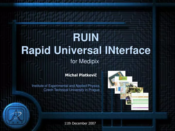
RUIN Rapid Universal INterface. for Medipix. April 2006 – half-time November 2006 – full-time. Work in UTEF. Work: RUIN – Rapid Universal INterface PCB for stepper motors control Prototype of USB1 modification for Timepix Spectroscopic modul ATLAS – Medipix wirring Measurement on PALS

E N D
RUIN Rapid Universal INterface for Medipix Michal Platkevič
April 2006 – half-time November 2006 – full-time Work in UTEF • Work: • RUIN – Rapid Universal INterface • PCB for stepper motors control • Prototype of USB1 modification for Timepix • Spectroscopic modul • ATLAS – Medipix wirring • Measurement on PALS • Measurement of slow neutrons in ILL • Diploma thesis (June 2007): • Signal processor controlled USB2.0 interface for Medipix2 detector • Presentations:USB2.0 Interface Status (CERN) • Signal processor controlled USB2.0 interface for Medipix2 detector (IWORID 9)Status of USB interfaces (MidSweden University) • Medipix /ATLAS – wiring (CERN) • Medipix in an extremely hostile environment (CERN) • USB2.0 interface for Medipix2 device (CERN) Michal Platkevič
Medipix2 detector MEDical Imaging PIXel detector of 2nd generation • Planarpixellateddetector (Si, GaAs, CdTe) is bump-bonded to read-out chip • Ionizing particle creates a charge in a sensitive volume • The charge is amplified and compared with a threshold • Digital counter is incremented. Bias Voltage • Pixels: 256 x 256 • Pixel size: 55 x 55 mm2 • Area: 1.5 x 1.5 cm2 (Si) + • Threshold level above • electronic noise • No false counting. Digital integration (counting) • No dark current. Unlimited dynamic range and exposure time. Detected count obeys poissonian distribution Amplifier Threshold level Compa- rator Counter: Particle count 000 001 Pixel electronics Pixel electronics Pixel electronics Michal Platkevič
Medipix – data read-out 256 pixels • The serial readout uses a LVDS port to shift out all the matrix data. • In readout mode the 14-bit shift register of each pixel is connected to the next one forming a 3584-bit shift register. • Communication between the pixel matrix and the IO logic is carried out through the 256-bit FSR. • The number of clocks needed in order to read one chip are 917512 (256x256x14+8). • External clock have to be used to shift the data from pixel to pixel. 3584-bit pixel column - 0 14-bit reg. 3584-bit pixel column - 1 14-bit reg. 3584-bit pixel column - 2 14-bit reg. 3584-bit pixel column - 254 14-bit reg. 3584-bit pixel column - 255 14-bit reg. bit bit bit … bit bit bit bit bit bit bit 14-bit reg. 14-bit reg. 14-bit reg. 14-bit reg. 14-bit reg. … … … … … … 14-bit reg. 14-bit reg. 14-bit reg. 14-bit reg. 14-bit reg. … 256 pixels … … … … … … … … … … … 14-bit reg. 14-bit reg. 14-bit reg. 14-bit reg. 14-bit reg. … bit bit bit bit bit 14-bit reg. 14-bit reg. 14-bit reg. 14-bit reg. 14-bit reg. bit bit bit bit bit … 256-bit FSR … … bit bit bit bit bit bit LVDS Input IO Logic LVDS Output 32-bit CMOS Output Michal Platkevič
Medipix chipboard PC and Powersupply USB2.0 Ethernet Powersupplies DSP FPGA Memory New Interface - Designstrategy New interface design puts emphasis on: • Speed of data read-out. (maximum speed possibility of the Medipix serial read-out: currently 200MHz) • Support for all chips of MPX family • Strategy: • Conecting with PC • USB2.0 - transfer rate of 480 Mb/s • 1Gb/s Ethernet • Usage of the digital signal processor • High data throughput • High computational performance (up to 8000 mips), even sophisticated data processing can be done here (threshold equalization, flat field correction, cluster analysis, data compression …) • Built in management of large memory • Usage of the FPGA • Hardware de-serialization of the serial data - decrease a processor load • I/O - LVDS, CMOS • Flexibility – possibility to change functionality without need of hardware modification New interface Michal Platkevič
Principle of Data Read-out • The serial data from the Medipix are shifted to fast shift registers • When the registers are filled up, the parallel data are loaded to the latch. • DSP reads the data from the latch via the data bus • Individual chips of multichip assembly are read out simultaneously. • Shift register is arranged as a 4 eight bit segments. Each segment can be fed from separate MPX chip. • Usage of multiple latches in form of FIFO could be advantageous Medipix Medipix Medipix Medipix LATCH LATCH LATCH LATCH Shift reg. Shift reg. Shift reg. Shift reg. Shift reg. Shift reg. Shift reg. Shift reg. Shift reg. Shift reg. Shift reg. Shift reg. 32 bits 32 bits 32 bits Shift reg. Shift reg. Shift reg. Shift reg. 32 bits PLL clock generator + control logic PLL clock generator + control logic PLL clock generator + control logic DSP DSP DSP 8 bits 8 bits 8 bits 8 bits 8 bits 8 bits 8 bits 8 bits 8 bits 8 bits 8 bits 8 bits PLL clock generator + control logic DSP 8 bits 8 bits 8 bits 8 bits Memory Memory Memory Memory USB 2.0 USB 2.0 USB 2.0 USB 2.0 Michal Platkevič
Status • Current prototype fully tested with MXR chip (up to 48 MHz) • Schematic design is finishing • PCB design will be ordered soon … FPGA evaluation board DSP evaluation board Power supply for Medipix Medipix Michal Platkevič
Power Power Power Flash DSP USB Memory DDR2 Header FPGA Cypress Memory DDR2 RJ45 DAC8x Ethernet ADC8x Interface Layout • Power supply PCB • For Medipix • For interface • Power connector • Logic • DSP (TI) • FPGA (Lattice) • USB (Cypress) • Ethernet (Intel) • DDR2 memory • Flash memory • Inner Connectors • JTAG for DSP • FPGA programming • General purpose • Power • Medipix • Power for Medipix • Connectors • Power • Mini USB • General purpose 20 pin header • Ethernet Changeable Medipix chipboard adapter To be more flexible we decided to use modular system Michal Platkevič
Power Power Interface Layout Power Flash USB Cypress DSP Memory DDR2 6 cm FPGA Memory DDR2 DAC8x RJ45 Ethernet ADC8x 14 cm Changeable chipboard adapter is recognized automatically and LVDS and CMOS pins of FPGA are configured. All signals from Medipix go via the FPGA (Lattice XP) with configurable inputs outputs – LVDS, CMOS Debugging Michal Platkevič
Supported Detectors • Read-out: • Serial • Parallel • Connecting: • Directly/via the cable • CMOS/LVDS • Detectors • Medipix2, Medipix MXR • Medipix Quad (daisy chain or separately) • Timepix • … Medipix3 Michal Platkevič
Serial data Control Data read-out and control Adapter board Medipix2, MXR, Timepix - 100 fps at 100 MHz FPGA DSP data bus 32 bits x 133 MHz 4.256 Gb/s Medipix chipboard Bank 2 LVDS 8pairs Bank 3 unused Bank 6 unused • LVDS - 6 pairs • Enable_OUT • Enable_IN • Data_OUT • Data_IN • Clk_IN • Clk_OUT • CMOS • 10 control bits Bank 7 CMOS 16b Michal Platkevič
Serial data Control Data read-out and control Standard Quad - 25 fps at 100 MHz FPGA DSP data bus 32 bits x 133 MHz 4.256 Gb/s Bank 2 LVDS 8pairs Bank 3 unused Bank 6 unused • LVDS - 6 pairs • Enable_OUT • Enable_IN • Data_OUT • Data_IN • Clk_IN • Clk_OUT • CMOS • 10 control bits Bank 7 CMOS 16b Michal Platkevič
Data read-out and control Quad – each chip read separately 100 fps at 100 MHz FPGA DSP data bus 32 bits x 133 MHz 4.256 Gb/s Bank 2 LVDS 8pairs Serial data Bank 3 LVDS 8pairs Serial data Serial data Bank 6 Serial data LVDS 8pairs Control Bank 7 CMOS 16b • LVDS - 24 pairs • 4 x Enable_OUT • 4 x Enable_IN • 4 x Data_IN • 4 x Data_OUT • 4 x Clk_IN • 4 x Clk_OUT • CMOS • 10 control bits Michal Platkevič
Data read-out and control • Medipix2, MXR, Timepix • parallel read-out • 3200 fps at 100 MHz FPGA DSP data bus 32 bits x 133 MHz 4.256 Gb/s Bank 2 LVDS 8pairs Serial data Bank 3 CMOS 16b Parallel data 32b Bank 6 CMOS 16b Control Bank 7 • LVDS - 5 pairs • Enable_OUT • Enable_IN • Data_IN • Clk_IN • Clk_OUT • CMOS • 10 control bits • Parallel data CMOS 16b Michal Platkevič
Data read-out and control 4 x standard Quad 25 fps at 100 MHz FPGA DSP data bus 32 bits x 133 MHz 4.256 Gb/s Bank 2 LVDS 8pairs Serial data Bank 3 LVDS 8pairs Serial data Serial data Bank 6 Serial data LVDS 8pairs Control Bank 7 CMOS 16b • LVDS - 24 pairs • 4 x Enable_OUT • 4 x Enable_IN • 4 x Data_IN • 4 x Data_OUT • 4 x Clk_IN • 4 x Clk_OUT • CMOS • 10 control bits Michal Platkevič
Finding name R • Rapid • Universal • INterface U IN RUIN Michal Platkevič
Thank you for your attention! Michal Platkevič