Download
1 / 14
140 likes | 329 Views
Pertemuan 8 Struktur Logik Gerbang CMOS-VLSI. Matakuliah : H0362/Very Large Scale Integrated Circuits Tahun : 2005 Versi : versi/01. Learning Outcomes. Pada Akhir pertemuan ini, diharapkan mahasiswa akan dapat menjelaskan struktur logik gerbang CMOS-VLSI. On device. nFET. A B F

E N D
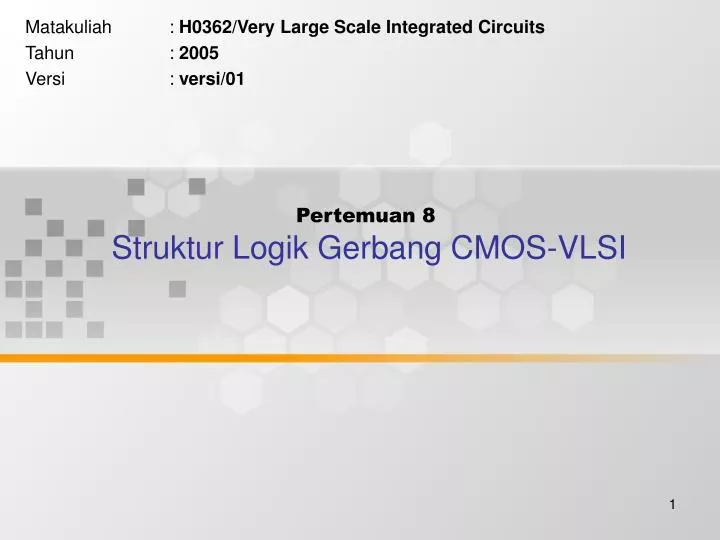
Pertemuan 8Struktur Logik Gerbang CMOS-VLSI Matakuliah : H0362/Very Large Scale Integrated Circuits Tahun : 2005 Versi : versi/01
Learning Outcomes Pada Akhir pertemuan ini, diharapkan mahasiswa akan dapat menjelaskan struktur logik gerbang CMOS-VLSI.
On device nFET A B F 0 0 0 0 1 1 1 0 1 1 1 0 A F pFET B pFET nFET F = A B Mirror Circuits Mirror circuits are based on series-parallel logic gates, but usually faster and have a more uniform layout
VDD VDD a a b b a b a a b b a b b a Gnd Rangkaian Layout Mirror Circuits
Rp Rp Rp Cp Rp Cp Cout Rn Rn Rn Cn Rn Cn : time constant r : rise time f : fall time Mirror Circuits
VDD + VSGp Pull-up Load - f VDD nFET Logic Array Pull-down p + VOL - Struktur umum pseudo nMOS + n VDD - Pseudo nMOS inverter Pseudo nMOS
En f Data VDD En f 0 Z 1 Data VDD Mp M1 En En f f En Data En M2 Data Mn Gnd Layout Rangkaian CMOS Tri-state Rangkaian Tri-state
1 time 1 time 0 T 2T Input valid VDD a b pFET c Hi-Z Hi-Z M1 f(a, b, c) + Cout M2 Vout - a Struktur clock gerbang CMOS b nFET c Clocked CMOS
VDD a b Mp VDD M1 a . b Cout M2 a Mn a b Out b Rangkaian NAND2 Gnd Layout Clocked CMOS
VDD f Mn a Cout Vout b nFET c d Evaluate Mp OFF Mn ON Precharge Mp ON Mn OFF Precharge Mp ON Mn OFF Mp T Basic dynamic gate logic Dynamic CMOS LOGIC A dynamic logic gate uses clocking and charge storage properties of MOSFETs to implement logic operations
Contoh rangkaian dynamic logik VDD VDD Mp f Cout Vout a b f c Mn Gnd c a b Layout Dynamic CMOS LOGIC
Dual Rail Logic We have been concentrating on single-rail logic Circuits where the value of a variables is eiher a 0 or 1 only. In dual-rail networks, both the variable x and its complement x are used to form the difference fx = (x – x )
VDD Vl Vr MP1 Latch MP2 f f VDD a a Sw2 Sw1 b Vl Vr b Logic tree c c a . b a . b a b a b AND / NAND Dual Rail Logic Structure of a CVSL logic gate
RESUME • Mirror Circuiuts. • Pseudo nMOS. • Tri-state. • Clocked CMOS. • Dynamic CMOS Logic. • Dual Rail Logic.