Download
1 / 84
840 likes | 846 Views
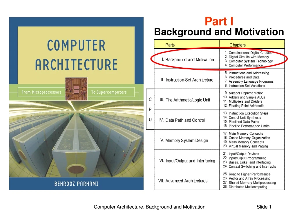
Part I Background and Motivation. I Background and Motivation. Provide motivation, paint the big picture, introduce tools: Review components used in building digital circuits Present an overview of computer technology Understand the meaning of computer performance

E N D
Part IBackground and Motivation Computer Architecture, Background and Motivation
I Background and Motivation • Provide motivation, paint the big picture, introduce tools: • Review components used in building digital circuits • Present an overview of computer technology • Understand the meaning of computer performance • (or why a 2 GHz processor isn’t 2 as fast as a 1 GHz model) Computer Architecture, Background and Motivation
1 Combinational Digital Circuits • First of two chapters containing a review of digital design: • Combinational, or memoryless, circuits in Chapter 1 • Sequential circuits, with memory, in Chapter 2 Computer Architecture, Background and Motivation
1.1 Signals, Logic Operators, and Gates Figure 1.1 Some basic elements of digital logic circuits, with operator signs used in this book highlighted. Computer Architecture, Background and Motivation
The Arithmetic Substitution Method z= 1 – z NOT converted to arithmetic form xy AND same as multiplication (when doing the algebra, set zk = z) xy = x + y-xyOR converted to arithmetic form xy = x + y- 2xy XOR converted to arithmetic form Example: Prove the identity xyz x y z?1 LHS = [xyz x] [y z] = [xyz + 1 – x – (1 – x)xyz] [1 – y + 1 – z – (1 – y)(1 – z)] = [xyz + 1 – x] [1 – yz] = (xyz + 1 – x) + (1 – yz) – (xyz + 1 – x)(1 – yz) = 1 + xy2z2 – xyz = 1 = RHS This is addition, not logical OR Computer Architecture, Background and Motivation
Variations in Gate Symbols Figure 1.2 Gates with more than two inputs and/or with inverted signals at input or output. Computer Architecture, Background and Motivation
Gates as Control Elements Figure 1.3 An AND gate and a tristate buffer act as controlled switches or valves. An inverting buffer is logically the same as a NOT gate. Computer Architecture, Background and Motivation
Wired OR and Bus Connections Figure 1.4 Wired OR allows tying together of several controlled signals. Computer Architecture, Background and Motivation
Control/Data Signals and Signal Bundles Figure 1.5 Arrays of logic gates represented by a single gate symbol. Computer Architecture, Background and Motivation
1.2 Boolean Functions and Expressions Ways of specifying a logic function Truth table: 2n row, “don’t-care” in input or output Logic expression: w (xyz), product-of-sums, sum-of-products, equivalent expressions Word statement: Alarm will sound if the door is opened while the security system is engaged, or when the smoke detector is triggered Logic circuit diagram: Synthesis vs analysis Computer Architecture, Background and Motivation
Manipulating Logic Expressions Table 1.2 Laws (basic identities) of Boolean algebra. Computer Architecture, Background and Motivation
Proving the Equivalence of Logic Expressions Example 1.1 Truth-table method: Exhaustive verification Arithmetic substitution xy = x + y-xy xy = x + y- 2xy Case analysis: two cases, x = 0 or x = 1 Logic expression manipulation Example: xy?xyxy x + y –2xy ?(1–x)y + x(1–y) –(1–x)yx(1–y) Computer Architecture, Background and Motivation
1.3 Designing Gate Networks AND-OR, NAND-NAND, OR-AND, NOR-NOR Logic optimization: cost, speed, power dissipation (xy) = xy Figure 1.6 A two-level AND-OR circuit and two equivalent circuits. Computer Architecture, Background and Motivation
Seven-Segment Display of Decimal Digits Optional segment Figure 1.7 Seven-segment display of decimal digits. The three open segments may be optionally used. The digit 1 can be displayed in two ways, with the more common right-side version shown. Computer Architecture, Background and Motivation
BCD-to-Seven-Segment Decoder Example 1.2 Figure 1.8 The logic circuit that generates the enable signal for the lowermost segment (number 3) in a seven-segment display unit. Computer Architecture, Background and Motivation
1.4 Useful Combinational Parts High-level building blocks Much like prefab parts used in building a house Arithmetic components (adders, multipliers, ALUs) will be covered in Part III Here we cover three useful parts: multiplexers, decoders/demultiplexers, encoders Computer Architecture, Background and Motivation
Multiplexers Figure 1.9 Multiplexer (mux), or selector, allows one of several inputs to be selected and routed to output depending on the binary value of a set of selection or address signals provided to it. Computer Architecture, Background and Motivation
Decoders/Demultiplexers Figure 1.10 A decoder allows the selection of one of 2a options using an a-bit address as input. A demultiplexer (demux) is a decoder that only selects an output if its enable signal is asserted. Computer Architecture, Background and Motivation
Encoders Figure 1.11 A 2a-to-a encoder outputs an a-bit binary number equal to the index of the single 1 among its 2a inputs. Computer Architecture, Background and Motivation
1.5 Programmable Combinational Parts A programmable combinational part can do the job of many gates or gate networks Programmed by cutting existing connections (fuses) or establishing new connections (antifuses) Programmable ROM (PROM) Programmable array logic (PAL) Programmable logic array (PLA) Computer Architecture, Background and Motivation
PROMs Figure 1.12 Programmable connections and their use in a PROM. Computer Architecture, Background and Motivation
PALs and PLAs Figure 1.13 Programmable combinational logic: general structure and two classes known as PAL and PLA devices. Not shown is PROM with fixed AND array (a decoder) and programmable OR array. Computer Architecture, Background and Motivation
1.6 Timing and Circuit Considerations Changes in gate/circuit output, triggered by changes in its inputs, are not instantaneous Gate delay d: a fraction of, to a few, nanoseconds Wire delay, previously negligible, is now important (electronic signals travel about 15 cm per ns) Circuit simulation to verify function and timing Computer Architecture, Background and Motivation
CMOS Transmission Gates Figure 1.15 A CMOS transmission gate and its use in building a 2-to-1 mux. Computer Architecture, Background and Motivation
2 Digital Circuits with Memory • Second of two chapters containing a review of digital design: • Combinational (memoryless) circuits in Chapter 1 • Sequential circuits (with memory) in Chapter 2 Computer Architecture, Background and Motivation
2.1 Latches, Flip-Flops, and Registers Figure 2.1 Latches, flip-flops, and registers. Computer Architecture, Background and Motivation
Reading and Modifying FFs in the Same Cycle Figure 2.3 Register-to-register operation with edge-triggered flip-flops. Computer Architecture, Background and Motivation
2.2 Finite-State Machines Example 2.1 Figure 2.4 State table and state diagram for a vending machine coin reception unit. Computer Architecture, Background and Motivation
Sequential Machine Implementation Figure 2.5 Hardware realization of Moore and Mealy sequential machines. Computer Architecture, Background and Motivation
2.3 Designing Sequential Circuits Example 2.3 Quarter in Final state is 1xx Dime in Figure 2.7 Hardware realization of a coin reception unit (Example 2.3). Computer Architecture, Background and Motivation
2.4 Useful Sequential Parts High-level building blocks Much like prefab closets used in building a house Other memory components will be covered in Chapter 17 (SRAM details, DRAM, Flash) Here we cover three useful parts: shift register, register file (SRAM basics), counter Computer Architecture, Background and Motivation
Figure 2.8 Register with single-bit left shift and parallel load capabilities. For logical left shift, serial data in line is connected to 0. Shift Register Computer Architecture, Background and Motivation
Register File and FIFO Figure 2.9 Register file with random access and FIFO. Computer Architecture, Background and Motivation
SRAM Figure 2.10 SRAM memory is simply a large, single-port register file. Computer Architecture, Background and Motivation
Binary Counter Figure 2.11 Synchronous binary counter with initialization capability. Computer Architecture, Background and Motivation
2.5 Programmable Sequential Parts A programmable sequential part contain gates and memory elements Programmed by cutting existing connections (fuses) or establishing new connections (antifuses) Programmable array logic (PAL) Field-programmable gate array (FPGA) Both types contain macrocells and interconnects Computer Architecture, Background and Motivation
PAL and FPGA Figure 2.12 Examples of programmable sequential logic. Computer Architecture, Background and Motivation
2.6 Clocks and Timing of Events Clock is a periodic signal: clock rate = clock frequency The inverse of clock rate is the clock period: 1 GHz 1 ns Constraint: Clock period tprop + tcomb + tsetup + tskew Figure 2.13 Determining the required length of the clock period. Computer Architecture, Background and Motivation
Synchronization Figure 2.14 Synchronizers are used to prevent timing problems arising from untimely changes in asynchronous signals. Computer Architecture, Background and Motivation
Level-Sensitive Operation Figure 2.15 Two-phase clocking with nonoverlapping clock signals. Computer Architecture, Background and Motivation
3 Computer System Technology • Interplay between architecture, hardware, and software • Architectural innovations influence technology • Technological advances drive changes in architecture Computer Architecture, Background and Motivation
3.1 From Components to Applications Figure 3.1 Subfields or views in computer system engineering. Computer Architecture, Background and Motivation
What Is (Computer) Architecture? Figure 3.2 Like a building architect, whose place at the engineering/arts and goals/means interfaces is seen in this diagram, a computer architect reconciles many conflicting or competing demands. Computer Architecture, Background and Motivation
3.2 Computer Systems and Their Parts Figure 3.3 The space of computer systems, with what we normally mean by the word “computer” highlighted. Computer Architecture, Background and Motivation
Price/Performance Pyramid Differences in scale, not in substance Figure 3.4 Classifying computers by computational power and price range. Computer Architecture, Background and Motivation
Automotive Embedded Computers Figure 3.5 Embedded computers are ubiquitous, yet invisible. They are found in our automobiles, appliances, and many other places. Computer Architecture, Background and Motivation
Personal Computers and Workstations Figure 3.6 Notebooks, a common class of portable computers, are much smaller than desktops but offer substantially the same capabilities. What are the main reasons for the size difference? Computer Architecture, Background and Motivation
Digital Computer Subsystems Figure 3.7 The (three, four, five, or) six main units of a digital computer. Usually, the link unit (a simple bus or a more elaborate network) is not explicitly included in such diagrams. Computer Architecture, Background and Motivation
3.3 Generations of Progress Table 3.2 The 5 generations of digital computers, and their ancestors. Computer Architecture, Background and Motivation
IC Production and Yield Figure 3.8 The manufacturing process for an IC part. Computer Architecture, Background and Motivation