Download

1 / 15
200 likes | 573 Views
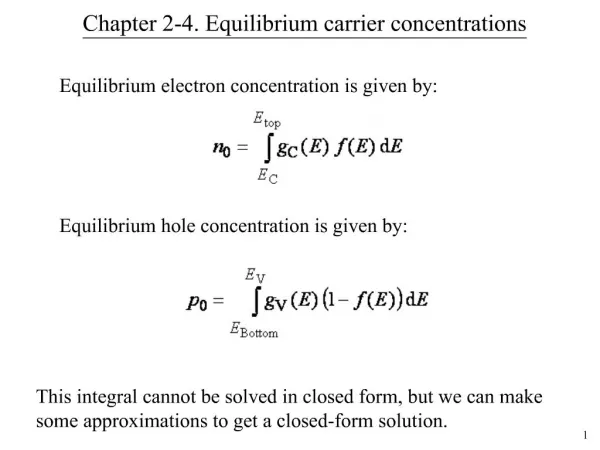
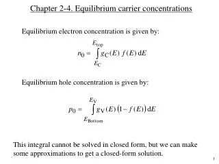
Chapter 2-4. Equilibrium carrier concentrations. Equilibrium electron concentration is given by:. Equilibrium hole concentration is given by:. This integral cannot be solved in closed form, but we can make some approximations to get a closed-form solution. Approximate solutions.

E N D
Chapter 2-4. Equilibrium carrier concentrations Equilibrium electron concentration is given by: Equilibrium hole concentration is given by: This integral cannot be solved in closed form, but we can make some approximations to get a closed-form solution.
Approximate solutions When ECEF > 3kT or EF < EC 3kT, the solution for the total free electron concentration can be expressed as: Eq 2.16a When EFEV > 3kT or EF > EV + 3kT, the solution for the total free hole concentration can be expressed as: Eq. 2.16b
Effective density of states Nc is called effective density of states in the conduction band Nv is called effective density of states in the valence band In Si: NC = 2.51 1019 (mn*/m0)3/2 cm3 = 2.8 1019 cm3 NV = 2.51 1019 (mp*/m0)3/2 cm3 = 1.0 1019 cm3 What do you get when you multiply n with p? The result gives an intrinsic property of the semiconductor.
Alternative expression for n and p Manipulation of the previous expressions will give us more useful expressions as given below: Note from previous class that: At T = 300K, ni = 2 106 cm3 in GaAs = 1 1010 cm3 in Si = 2 1013 cm3 in Ge An intrinsic property
Show that Hint: Start with Eq. 2.16 in text
Charge neutrality relationship So far, we haven’t discussed any relationship between the dopant concentration and the free carrier concentrations. Charge neutrality condition can be used to derive this relationship. The net charge in a small portion of a uniformly doped semiconductor should be zero. Otherwise, there will be a net flow of charge from one point to another resulting in current flow (that is against out assumption of thermal equilibrium). Charge/cm3 = q p – q n + q ND+q NA = 0 or p – n + ND+ NA = 0 where ND+ = # of ionized donors/cm3 and NA = # of ionized acceptors per cm3. Assuming total ionization of dopants, we can write:
Carrier concentration calculations Assume a non-degenerately doped semiconductor and assumetotal ionization of dopants. Then, n p = ni2 ; electron concentration hole concentration = ni2 pn + NDNA = 0; net charge in a given volume is zero. Solve for n and p in terms of ND and NA We get: (ni2 / n) n + NDNA = 0 n2n (NDNA) ni2 = 0 Solve this quadratic equation for the free electron concentration, n. From n p = ni2 equation, calculate free hole concentration, p.
Special cases • Intrinsic semiconductor: ND= 0 and NA = 0 p = n = ni • Doped semiconductors where | ND NA | >> ni n = NDNA ; p = ni2 / n if ND > NA p = NAND ; n = ni2 / p if NA > ND • Compensated semiconductor n = p = ni when ni >> | ND NA | When | ND NA | is comparable to ni,, we need to use the charge neutrality equation to determine n and p.
Equations to remember Note: Our interest was in determining n and p. Free carriers strongly influence the properties of semiconductors.
Example 1 (a) Consider Si doped with 1014 cm3 boron atoms. Calculate the carrier concentration (n and p) at 300 K. (b) Determine the position of the Fermi level and plot the band diagram. (c) Calculate the the carrier concentration (n and p) in this Si material at 470 K. Assume that intrinsic carrier concentration at 470 K in Si is 1014 cm3. (Refer to figure 2.20). (d) Determine the position of the Fermi level with respect to Ei at 470 K.
Example 2 Consider a Si sample doped with 3 1016 cm3 of phosphorous (P) atoms and 1016 cm3 of boron (B) atoms. (a) Is the semiconductor n-type or p-type? (b) Determine the free carrier concentration (hole and electron concentrations, or p and n) at 300K. (c) Determine the position of the Fermi level and draw the band diagram.