Download
1 / 7
80 likes | 112 Views
Device Design: Stage 2 (Modified Microchannel Design). Device Objective To test the viability of a two-level passive micro-fluidic device Modifications from Stage 1 Moved reservoir positions to fit existing packaging

E N D
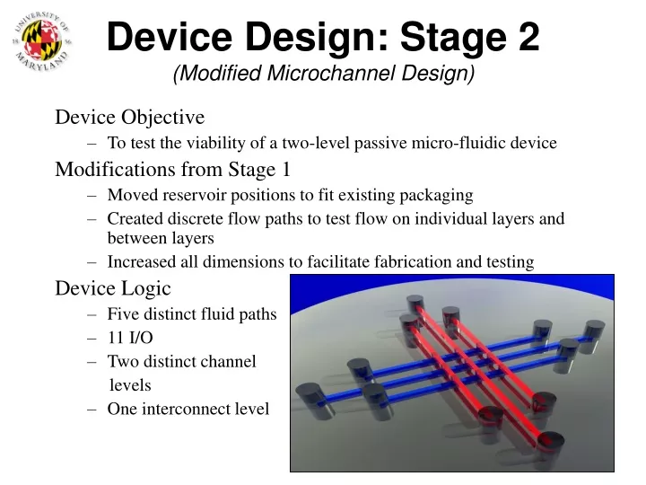
Device Design: Stage 2(Modified Microchannel Design) Device Objective • To test the viability of a two-level passive micro-fluidic device Modifications from Stage 1 • Moved reservoir positions to fit existing packaging • Created discrete flow paths to test flow on individual layers and between layers • Increased all dimensions to facilitate fabrication and testing Device Logic • Five distinct fluid paths • 11 I/O • Two distinct channel levels • One interconnect level
Device Design: Stage 2(Modified Microchannel Design) Device Geometry • Chosen for process compatibility • Rectangular micro-channels • Square Interconnects • Circular reservoirs Materials • All PDMS layers on a Silicon substrate with SU8 for mold creation • Heightened design flexibility • PDMS biocompatibility • Equipment and material availability and fast turnaround time
Micro-Channel Layer 1 Interconnect Layer Micro-Channel Layer 2 Device Design: Stage 2(Modified Microchannel Design) Process Sequence and Mask Design • Begin with three polished Si wafers • Spin SU-8 (negative photoresist) on the Si wafers and pre-bake at 95°C • Align each of the three wafers with one of the three masks shown below and expose the SU-8 to ultraviolet light, then post-bake at 95°C • Develop the SU8 so that the unexposed areas are removed • Results in three distinct SU8 molds
Device Design: Stage 2(Modified Microchannel Design) 5. Spin PDMS on the SU8 molds less than the vertical dimension of the SU-8 protrusions • Mix PDMS (Sylgard 184, Dow-Corning) 10:1 with curing agent • Spin on PDMS • Dip the Si wafer in a sodium dodecyl sulfate(SDS) adhesion barrier and allow it to dry naturally • Bake in box furnace for 2 hours at 70°C 6. Delaminate and stack all three PDMS layers in the following order: Micro-channel Layer 1, Interconnect Layer, Micro-channel layer 2
Device Design: Stage 2(Modified Microchannel Design) Final Expected Result:
Rr + Rc + Ri + Rv RTotal Device Design: Stage 3(Pressure Actuated Valve Design) Fluid Flow Modeling • Assumed Fluid Flow Rate based on Fluid velocity • Based on literature search: 1500 cm/minute= 2.5 E5 μm/sec • 1.25 E 10 μm3/sec= 0.0125 cm3/sec • Fluidic Resistance: R= ΔP/Q [(N*s)/m5] • R(circular cross section)= 8μL/(πr4) • μ= Fluid Viscosity= 0.01 g/sec*cm • L= Length of channel • r= Radius of channel • R(Rectangular cross section)~ 12μL/(wh3) • w= Width of the channel • h= Height of the Channel • Total Fluidic Resistance = Rr + Rc + Ri + Rv
Device Design: Stage 3(Pressure Actuated Valve Design) Fluid Flow Modeling • Determined the velocity, fluidic resistance, Reynolds number and pressure gradient in each section of the fluids path and found the relevant total fluid path properties Sample output for the two valve fluid path • Total Pressure Gradient • ~15330Pa~115 Torr • Pressure Gradient at the Valve • 3750 Pa~28 Torr • Fluid Flow Rate • 1.25 E 10 μm3/sec= 0.0125 cm3/sec • Total Cycle Time • ~21.2 seconds