Download
1 / 25
250 likes | 410 Views
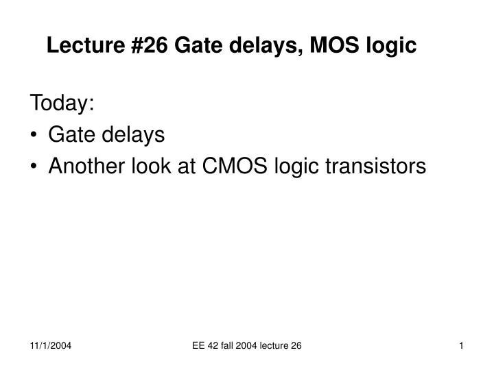
Lecture #26 Gate delays, MOS logic. Today: Gate delays Another look at CMOS logic transistors. V DD = 3V. V IN =3V. +. V OUT. R N. -. t D. V SS = 0V. V OUT. Output when:. V DD = 3V. V IN jumps from 3V to 0V. -. R P. 3. V IN =0V. +. V IN jumps from 0V to 3V. V OUT.

E N D
Lecture #26 Gate delays, MOS logic Today: • Gate delays • Another look at CMOS logic transistors EE 42 fall 2004 lecture 26
VDD = 3V VIN =3V + VOUT RN - tD VSS = 0V VOUT Output when: VDD = 3V VIN jumps from 3V to 0V - RP 3 VIN =0V + VIN jumps from 0V to 3V VOUT 0 t - - VSS = 0V Controlled Switch Model of Inverter What is the gate delay tD for this simple inverter? If we define tD as the time to go halfway to the asymtotic limit, tD = 0.69RC . To get equal delays we will need to set RP = RN. EE 42 fall 2004 lecture 26
v ( t ) Ideal Logic gate R Ideal Logic gate OUT VX etc. C Model of Actual Logic Gate vIN vOUT VX t tD = 0. 69 RC Simple model for logic delays (slide 2 again) We model actual logic gate as an ideal logic gate fed by an RC network which represents the dominant R and C in the gate. This model is very close to real physics: the transistors are inherently extremely fast, but are slowed by the need to charge up (or discharge) the capacitance at the various nodes. EE 42 fall 2004 lecture 26
VDD A C B VOUT B A C Logic is Complementary and produces F = A + (BC) CMOS Logic Gate NMOS and PMOS use the same set of input signals PMOS only in pull-up PMOS conduct when input is low PMOS do not conduct when A +(BC) NMOS only in pull-down NMOS conduct when input is high. NMOS conduct for A + (BC) EE 42 fall 2004 lecture 26
VDD A C B VOUT B A C CMOS Logic Gate: Example Inputs A = 0 B = 0 C = 0 PMOS all conduct Output is High = VDD NMOS do not conduct Logic is Complementary and produces F = 1 EE 42 fall 2004 lecture 26
VDD A C B VOUT B A C CMOS Logic Gate: Example Inputs A = 0 B = 1 C = 1 PMOS A conducts; B and C Open Output is High = 0 NMOS B and C conduct; A open Logic is Complementary and produces F = 0 EE 42 fall 2004 lecture 26
VDD VDD A RD RD RU RD RU RU A C B VOUT C B VOUT B A B A C C Switched Equivalent Resistance Network Switches close when input is low. Switches close when input is high. EE 42 fall 2004 lecture 26
VDD A RD RD RU RU RU RD C B VOUT B A COUT = 50 fF C Logic Gate Propagation Delay: Initial State The initial state depends on the old (previous) inputs. The equivalent resistance of the pull-down or pull-up network for the transient phase depends on the new (present) input state. Example: A=0, B=0, C=0 for a long time. These inputs provided a path to VDD for a long timeand the capacitor has charged up to VDD = 5V. EE 42 fall 2004 lecture 26
VDD A RU RD RD RD RU RU And opens apath from VOUT to GND C B VOUT B A COUT = 50 fF C Logic Gate Propagation Delay: Transient At t=0, B and C switch from low to high (VDD) and A remains low. This breaks the path from VOUT to VDD COUT discharges through the pull-down resistance of gates B and C in series. Dt = 0.69(RDB+RDC)COUT = 0.69(20kW)(50fF) = 690 ps The propagation delay is two times longer than that for the inverter! EE 42 fall 2004 lecture 26
VDD RD RD RU RU RU RD A Fastest overall? C B VOUT Slowest overall? B COUT = 50 fF A C Logic Gate: Worst Case Scenarios What combination of previous and present logic inputs will make the Pull-Up the fastest? What combination of previous and present logic inputs will make the Pull-Up the slowest? What combination of previous and present logic inputs will make the Pull-Down the fastest? What combination of previous and present logic inputs will make the Pull-Down the slowest? EE 42 fall 2004 lecture 26
MOS transistors • The heart of digital logic is the MOS transistor, both NMOS and PMOS • In the next couple of lectures, we will learn more about how CMOS logic works at the circuit level, • starting with a review of the NMOS transistor EE 42 fall 2004 lecture 26
n n “Metal” gate (Al or Si) gate oxide insulator P-type Silicon NMOS TRANSISTOR STRUCTURE NMOS = N-channel Metal Oxide Silicon Transistor An insulated gate is placed above the silicon Its purpose is to control the current between n-type regions (by inducing a “channel” of electrons when a positive V is applied). EE 42 fall 2004 lecture 26
“Semiconductor” “Metal” “Oxide” G D S n n “Metal” gate (Al or Si) P gate oxide insulator MOS TRANSISTOR STRUCTURE DEVICE IN CROSS-SECTION The “gate” electrode is just a conductor to act as the capacitor top plate The lower “body” electrode is silicon with almost no electrons present (essentially an insulator) Thus no current can flow between the D and S electrodes which contact the silicon EE 42 fall 2004 lecture 26
+ 5V - G D S + + + + + + + + + + + + n n _ _ _ _ _ _ _ _ _ _ _ _ “Metal” gate (Al or Si) P oxide insulator MOS TRANSISTOR STRUCTURE DEVICE with + Gate Voltage Here the 5V across the capacitor induces + charge on the gate and – charge on the surface of the semiconductor, according to Q=CV. The charge in the semiconductor is really just free electrons which can carry current (just like the electrons in a metal can carry current). Thus by applying a voltage to the gate we have provided a conduction path for current if a voltage is applied from D to S. EE 42 fall 2004 lecture 26
i G iD S D + VGS oxide Si + VDS tox VDS VGS >> VT VGS > VT iD Zero if VGS is small MOS Transistor as a controlled switch But the device is not fundamentally ON/OFF. As VGS increases, the switch resistance decreases (slope becomes steeper). Thus we have a “family of I-V curves” which describe the current into D as a function of both VDS and VGS EE 42 fall 2004 lecture 26
ID 3-Terminal Device D G ID versus VDS for VGS = 2V. +- VGS S ID (mA) 10 VDS (V) 1 2 Three-Terminal Device Graphs Concept of 3-Terminal Device Graphs: We set a voltage (or current) at one set of terminals (here we will apply a fixed VGS of 2V) and conceptually draw a box around the device with only two terminals emerging So we can now plot the two-terminal characteristic (here ID versus VDS). EE 42 fall 2004 lecture 26
ID 3-Terminal Device D G VGS = 3 + - VGS = 2 VGS S ID (mA) 10 VGS = 1 VDS (V) 1 2 Three-Terminal Parametric Graphs Concept of 3-Terminal Parametric Graphs: We set a voltage (or current) at one set of terminals (here we will apply a fixed VGS) and conceptually draw a box around the device with only two terminals emerging so we can again plot the two-terminal characteristic (here ID versus VDS). But we can do this for a variety of values of VGS with the result that we get a family of curves. EE 42 fall 2004 lecture 26
ID VGS iD G + + VGS = 2 S D VDS VGS = 1.5 VGS VGS = 1 VGS = 0 VDS NMOS I vs V Characteristics Example of experimental I-V characteristics. (You can do in the 43 Lab) For low gate voltages, no drain current flows. As VGS is increased above threshold, e.g. 1V, the nonlinear “saturating” I-V curve is obtained. Increasing VGS causes ID to increase, as the family of curves indicates. EE 42 fall 2004 lecture 26
ID(mA) 1.25 4 3 2 1 0.75 0.5 VDS 0 0.5 The Family of ID vs VGS Curves For short-channel devices used in digital logic, the ID vs VDS curves are decidedly nonlinear! Curves which start out as simple linear resistors saturate as shown on this and the previous slide. We can approximate the I-V characteristics as two straight lines. a) the linear “resistance” region at low VDS and b) the saturation region (almost horizontal) at larger VDS. EE 42 fall 2004 lecture 26
ID IDS D D G VDD ID RDN G S Electrical Model S VDS NMOS Summary ID for VGS = maximum (VDD) If VGS = 0. N Ch The circuit symbol A value for RDN is chosen to give the correct timing delay. EE 42 fall 2004 lecture 26
VDD = 3V VIN =3V + VOUT RN - VSS = 0V ID VGS = VDD - IDS When VGS jumps to VDD, the current jumps from zero to this value. VGS = 0 VDS VDD VDD/2 Remember the Role of the Switch The NMOS transistor conducts the charge out of the capacitor to ground when its input (VGS) is high (VDD). We cover up the non-useful parts of the circuit for simplicity. G D The capacitor was initially at 3V (VDD), and goes toward zero. We define one stage delay by the time for VOUT = VDS to reach 1.5V (VDD /2). S Now lets draw the I-V characteristics of the NMOS As the capacitor discharges, V decreases and the current follows the IDS vs VDS curve. As a first approximation we will assume that l=0 EE 42 fall 2004 lecture 26
G D + - + VIN =3V C VOUT RN - S - We integrate the capacitor equation to find the time: ID VGS = VDD IDS As the capacitor discharges, V decreases and the current follows the IDS vs VDS curve. VGS = 0 VDS VDD VDD/2 Computing the stage delay The stage delay is the time for VOUT to decrease from VDD to VDD /2. The capacitor is initially charged to 3V, and we want to see how long it takes to reach 1.5V. That is the delay. As V goes from VDD to VDD /2, the average current IAV IDS( 1+lX(3/4)VDD) ( IDS if l is close to zero; consider this case first). =CVDD/2IDS for l = 0 EE 42 fall 2004 lecture 26
G D + - + VIN =3V C VOUT RN - S - ID VGS = VDD IDS Here we approximate l = 0 so the slope is zero VGS = 0 VDS VDD VDD/2 Computing the stage delay (for l0) The stage delay t is the time for VOUT to decrease from VDD to VDD /2. Thus t = CVDD/2IDS for l = 0 Now suppose we had instead assumed a resistance which averaged VDD/IDS and VDD/2IDS ,that is 3VDD/4IDS , shown as the blue line in the figure below. We would compute t = 0.69RC = 0.69 (3VDD/4IDS )C That is t = 0.52 CVDD/IDS which is only 4% larger than the value we found by doing the actual integration. EE 42 fall 2004 lecture 26
We found by integration that G D + - + VIN =3V C VOUT RN - S - ID VGS = VDD IDS As the capacitor discharges, VOUT decreases and the current follows the IDS vs VDS curve. VGS = 0 VDS VDD VDD/2 Computing the stage delay (for l>0) Since IAV IDS( 1+lX(3/4)VDD) we have t =0.5C VDD / IDS( 1+lX(3/4)VDD). Now lets compare with the value we would get using an averaged-value resistor (blue line below) As VOUT goes from VDD to VDD /2, the average resistance is (3/4) VDD /IDS( 1+lX(3/4)VDD) thus our time constant (0.69RC) equals • =0.69 C (3/4) VDD /IDS( 1+lX(3/4)VDD) = 0.52 C VDD /IDS ( 1+lX(3/4)VDD) Again, this is only 4% different from the answer obtained by direct integration EE 42 fall 2004 lecture 26
G D + - + VIN =3V C VOUT RN - S D - IDS ( 1+lVDD) G ID RDN VGS = VDD S Electrical Model IDS VGS = 0 VDS VDD VDD/2 Computing the stage delay - Summary During the discharge of C through the NMOS transistor, we have shown that we can compute the stage delay t by using the switch model with an effective resistance RDN = (3/4) VDD /IDS( 1+lX(3/4)VDD) Thus we can compute the stage delay, 0.69RDNC, EE 42 fall 2004 lecture 26