Download
1 / 1
10 likes | 105 Views
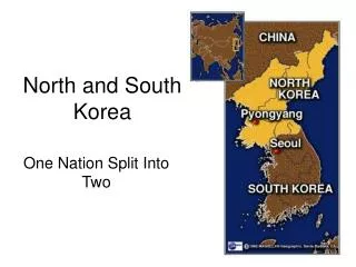
SEMINAR. 1 . T itle : Introduction to Nanotechnology Policy in Korea 2. S peaker : D eputy Director WooJin Lee (Ministry of Science & Technology) 3. T ime : 1 6 :00 – 17:30, Tuesday, June 13, 2006

E N D
SEMINAR 1. Title : Introduction to Nanotechnology Policy in Korea 2. Speaker : Deputy Director WooJin Lee (Ministry of Science & Technology) 3. Time : 16:00 – 17:30, Tuesday, June13, 2006 4. Place : e+ Lecture Hall (room 83188), 2nd Research Building, Sungkyunkwan University 5. Summary : As an innovative administration system for science and technology (S&T) in Korea, the office of S&T innovation (OSTI) has been established within the ministry of science and technology (MOST) in October 2004. In this presentation, the main missions of OSTI will be introduced as a pan-ministerial coordinating organization for S&T policies: coordination for all S&T policies related to industries, manpower and regions; strategic allocation and distribution of national R&D budget; impartial evaluation of all R&D programs. Especially, the current governmental efforts on nanotechnology as a national leading technology will be explained here in terms of R&D planning, budget and policies. 6 Background : Education 1994 Metallurgical Engineering, Hanyang University, B.S 1996 Materials Science, Korea Advanced Institute of Science and Technology, M.S 2000 Materials Science, Korea Advanced Institute of Science and Technology, Ph.D Work Experience 2000-2002 Senior Research Staff, Hynix Semiconductor Inc. - Advanced electronic packaging process for DRAM - Process development of chemical mechanical planarization (CMP) 2002-2004 Post-doctoral Associate, Chemical Engineering, University of Minnesota, - Oxide (TiO2&ZrO2) nanotube formation using electrochemical anodization - Nanoscale measurement using SPM(AFM & NSOM) 2004- Metallurgical Deputy Director, Coordinating division for Machinery and Materials in OSTI, MOST Sungkyunkwan University