Download
1 / 27
280 likes | 499 Views
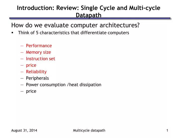
Introduction: Review: Single Cycle and Multi-cycle Datapath. How do we evaluate computer architectures? Think of 5 characteristics that differentiate computers Performance Memory size Instruction set price Reliability Peripherals Power consumption /heat dissipation price.

E N D
Introduction: Review: Single Cycle and Multi-cycle Datapath How do we evaluate computer architectures? • Think of 5 characteristics that differentiate computers • Performance • Memory size • Instruction set • price • Reliability • Peripherals • Power consumption /heat dissipation • price Multicycle datapath
Single-Cycle Performance • In CMPE 325 we saw a MIPS single-cycle datapath and control unit. • In CMPE 421, we’ll explore factors that contribute to a processor’s execution time, and specifically at the performance of the single-cycle machine. • AND we’ll explore how to improve on the single cycle machine’s performance using pipelining.
Three Components of CPU Performance Performance
Instructions Executed • Instructions executed: • not interested in the static instruction count, or how many lines of code are in a program. • Instead, the dynamic instruction count, or how many instructions are actually executed when the program runs. • There are three lines of code below, but the number of instructions executed would be 2001. li $a0, 1000 BACK: sub $a0, $a0, 1 bne $a0, $0, BACK CPU timeX,P = Instructions executedP * CPIX,P * Clock cycle timeX Cycles Per Instruction Performance
CPI • The average number of clock cycles per instruction, or CPI, is a function of the machineandprogram. • The CPI depends on the actual instructions appearing in the program—a floating-point intensive application might have a higher CPI than an integer-based program. • It also depends on the CPU implementation. For example, a Pentium can execute the same instructions as an older 80486, but faster. • Remember In CMPE325, we assumed each instruction took one cycle, so we had CPI = 1. • The CPI can be >1 due to memory stalls and slow instructions. • The CPI can be <1 on machines that execute more than 1 instruction per cycle (superscalar, Duo Core, Quad core). Performance
Clock cycle time • One “cycle” is the minimum time it takes the CPU to do any work. • The clock cycle time or clock period is just the length of a cycle. • The clock rate, or frequency, is the reciprocal of the cycle time. • Generally, a higher frequency is better. • Some examples illustrate some typical frequencies. • A 500MHz processor has a cycle time of 2ns. • A 2GHz (2000MHz) CPU has a cycle time of just 0.5ns (500ps). Performance
Execution time, again CPU timeX,P = Instructions executedP * CPIX,P * Clock cycle timeX • The easiest way to remember this is match up the units: • Make things faster by making any component smaller!! • Often easy to reduce one component by increasing another Performance
Example 1: ISA-compatible processors • Let’s compare the performances two x86-based processors. • An 800MHz AMD Duron, with a CPI of 1.2 for an MP3 compressor. • A 1GHz Pentium III with a CPI of 1.5 for the same program. • Compatible processors implement identical instruction sets and will use the same executable files, with the same number of instructions. • But they implement the ISA differently, which leads to different CPIs. CPU timeAMD,P = InstructionsP * CPIAMD,P * Cycle timeAMD = = N x1.2x1/800=3/2000 CPU timeP3,P = InstructionsP * CPIP3,P * Cycle timeP3 = = Nx1/5x1/1000=3/2000 Performance
0 M u x 1 1 M u x 0 Add Add Shift left 2 4 PCSrc RegWrite MemToReg MemWrite I [25 - 21] Read address Instruction [31-0] Read register 1 Read data 1 PC ALU Read address Read data I [20 - 16] Zero Read register 2 Instruction memory Read data 2 Result Write address 0 M u x 1 0 M u x 1 Write register Data memory Write data Registers I [15 - 11] ALUOp Write data MemRead ALUSrc RegDst Sign extend I [15 - 0] The single-cycle design from last time A control unit (not shown) generates all the control signals from the instruction’s “op” and “func” fields. Multicycle datapath
The example add from last time • Consider the instruction add $s4, $t1, $t2. • Assume $t1 and $t2 initially contain 1 and 2 respectively. • Executing this instruction involves several steps. • The instruction word is read from the instruction memory, and the program counter is incremented by 4. • The sources $t1 and $t2 are read from the register file. • The values 1 and 2 are added by the ALU. • The result (3) is stored back into $s4 in the register file. Multicycle datapath
Instruction execution review Multicycle datapath
RegWrite MemToReg MemWrite Read address Instruction [31-0] I [25 - 21] Read register 1 Read data 1 ALU Read address Read data 1 M u x 0 I [20 - 16] Zero Read register 2 Instruction memory Read data 2 0 M u x 1 Result Write address 0 M u x 1 Write register Data memory Write data Registers I [15 - 11] ALUOp Write data MemRead ALUSrc RegDst I [15 - 0] Sign extend Example: Instruction Fetch (IF) • Let’s quickly review how lw is executed in the single-cycle datapath. • We’ll ignore PC incrementing and branching for now. • In the Instruction Fetch (IF) step, we read the instruction memory. Pipelining
RegWrite MemToReg MemWrite Read address Instruction [31-0] I [25 - 21] Read register 1 Read data 1 ALU Read address Read data 1 M u x 0 I [20 - 16] Zero Read register 2 Instruction memory Read data 2 0 M u x 1 Result Write address 0 M u x 1 Write register Data memory Write data Registers I [15 - 11] ALUOp Write data MemRead ALUSrc RegDst I [15 - 0] Sign extend Instruction Decode (ID) • The Instruction Decode (ID) step reads the source register from the register file. Pipelining
RegWrite MemToReg MemWrite Read address Instruction [31-0] I [25 - 21] Read register 1 Read data 1 ALU Read address Read data 1 M u x 0 I [20 - 16] Zero Read register 2 Instruction memory Read data 2 0 M u x 1 Result Write address 0 M u x 1 Write register Data memory Write data Registers I [15 - 11] ALUOp Write data MemRead ALUSrc RegDst I [15 - 0] Sign extend Execute (EX) • The third step, Execute (EX), computes the effective memory address from the source register and the instruction’s constant field. Pipelining
RegWrite MemToReg MemWrite Read address Instruction [31-0] I [25 - 21] Read register 1 Read data 1 ALU Read address Read data 1 M u x 0 I [20 - 16] Zero Read register 2 Instruction memory Read data 2 0 M u x 1 Result Write address 0 M u x 1 Write register Data memory Write data Registers I [15 - 11] ALUOp Write data MemRead ALUSrc RegDst I [15 - 0] Sign extend Memory (MEM) • The Memory (MEM) step involves reading the data memory, from the address computed by the ALU. Pipelining
Writeback (WB) • Finally, in the Writeback (WB) step, the memory value is stored into the destination register. RegWrite MemToReg MemWrite Read address Instruction [31-0] I [25 - 21] Read register 1 Read data 1 ALU Read address Read data 1 M u x 0 I [20 - 16] Zero Read register 2 Instruction memory Read data 2 0 M u x 1 Result Write address 0 M u x 1 Write register Data memory Write data Registers I [15 - 11] ALUOp Write data MemRead ALUSrc RegDst I [15 - 0] Sign extend Pipelining
0 M u x 1 1 M u x 0 Add Add Shift left 2 PCSrc=0 MemToReg=0 MemWrite Read address Instruction [31-0] Read register 1 Read data 1 PC ALU Read address Read data Zero Read register 2 Instruction memory Read data 2 Write address Result 0 M u x 1 0 M u x 1 Write register Data memory Write data Registers ALUOp =ADD Write data MemRead ALUSrc=0 RegDst =1 Sign extend I [15 - 0] How the add goes through the datapath PC+4 4 RegWrite=1 I [25 - 21] 01001 00...01 I [20 - 16] 01010 00...10 I [15 - 11] 10100 00...11 Multicycle datapath
Performance of Single-cycle Design CPU timeX,P = Instructions executedP * CPIX,P * Clock cycle timeX Performance
MemWrite Read register 1 Read data 1 PC Read address Read data Read register 2 RegWrite Read data 2 Write address Write register Data memory Write data Registers Write data MemRead Edge-triggered state elements • In an instruction like add $t1, $t1, $t2, how do we know $t1 is not updated until after its original value is read? • We’ll assume that our state elements are positive edge triggered, and are updated only on the positive edge of a clock signal. • The register file and data memory have explicit write control signals, RegWrite and MemWrite. These units can be written to only if the control signal is asserted and there is a positive clock edge. • In a single-cycle machine the PC is updated on each clock cycle, so we don’t bother to give it an explicit write control signal. Multicycle datapath
The datapath and the clock • On a positive clock edge, the PC is updated with a new address. • A new instruction can then be loaded from memory. The control unit sets the datapath signals appropriately so that • registers are read, • ALU output is generated, • data memory is read or written, and • branch target addresses are computed. • Several things happen on the next positive clock edge. • The register file is updated for arithmetic or lw instructions. • Data memory is written for a sw instruction. • The PC is updated to point to the next instruction. • In a single-cycle datapath everything in Step 2 must complete within one clock cycle,before the next positive clock edge. How long is that clock cycle? Multicycle datapath
0 M u x 1 1 M u x 0 Add Add Shift left 2 PCSrc MemToReg MemWrite Read address Instruction [31-0] Read register 1 Read data 1 PC ALU Read address Read data Zero Read register 2 Instruction memory Read data 2 Write address Result 0 M u x 1 0 M u x 1 Write register Data memory Write data Registers ALUOp Write data MemRead ALUSrc RegDst Sign extend I [15 - 0] Compute the longest path in the add instruction PC+4 4 2 ns 2 ns RegWrite 0 ns I [25 - 21] I [20 - 16] 2 ns I [15 - 11] 0 ns 2 ns 1 ns 0 ns 0 ns 2 ns Multicycle datapath
1 M u x 0 I [25 - 21] Read address Instruction [31-0] Read register 1 Read data 1 ALU Read address Read data I [20 - 16] Zero Read register 2 Instruction memory Read data 2 Result Write address 0 M u x 1 0 M u x 1 Write register Data memory Write data Registers I [15 - 11] Write data Sign extend I [15 - 0] The slowest instruction... • If all instructions must complete within one clock cycle, then the cycle time has to be large enough to accommodate the slowest instruction. • For example, lw $t0, –4($sp) is the slowest instruction needing __ns. • Assuming the circuit latencies below. 2 ns 2 ns 0 ns 2 ns 0 ns 0 ns 1 ns 0 ns Multicycle datapath
1 M u x 0 reading the instruction memory 2ns reading the base register $sp 1ns computing memory address $sp-4 2ns reading the data memory 2ns storing data back to $t0 1ns I [25 - 21] 8ns Read address Instruction [31-0] Read register 1 Read data 1 ALU Read address Read data I [20 - 16] Zero Read register 2 Instruction memory Read data 2 Result Write address 0 M u x 1 0 M u x 1 Write register Data memory Write data Registers I [15 - 11] Write data Sign extend I [15 - 0] The slowest instruction... • If all instructions must complete within one clock cycle, then the cycle time has to be large enough to accommodate the slowest instruction. • For example, lw $t0, –4($sp) needs 8ns, assuming the delays shown here. 2 ns 2 ns 0 ns 2 ns 0 ns 0 ns 1 ns 0 ns Multicycle datapath
1 M u x 0 reading the instruction memory 2 ns reading registers $t1 and $t2 1 ns computing $t1 + $t2 2 ns storing the result into $s0 1 ns 6 ns I [25 - 21] Read address Instruction [31-0] Read register 1 Read data 1 ALU Read address Read data I [20 - 16] Zero Read register 2 Instruction memory Read data 2 Result Write address 0 M u x 1 0 M u x 1 Write register Data memory Write data Registers I [15 - 11] Write data 2 ns Sign extend 2 ns 0 ns 2 ns I [15 - 0] 0 ns 0 ns 1 ns 0 ns ...determines the clock cycle time • If we make the cycle time 8ns then every instruction will take 8ns, evenif they don’t need that much time. • For example, the instruction add $s4, $t1, $t2 really needs just 6ns. Multicycle datapath
How bad is this? • With these same component delays, a sw instruction would need 7ns, and beq would need just 5ns. • Let’s consider the gcc instruction mix from the textbook. • With a single-cycle datapath, each instruction would require 8ns. • But if we could execute instructions as fast as possible, the average time per instruction for gcc would be: (48% x 6ns) + (22% x 8ns) + (11% x 7ns) + (19% x 5ns) = 6.36ns • The single-cycle datapath is about 1.26 times slower! Multicycle datapath
Review of a Multiple Cycle Implementation • The root of the single cycle processor’s problems: • The cycle time has to be long enough for the slowest instruction • Solution: • Break the instruction into smaller steps • Execute each step (instead of the entire instruction) in one cycle • Cycle time: time it takes to execute the longest step • Keep all the steps to have similar length • This is the essence of the multiple cycle processor • The advantages of the multiple cycle processor: • Cycle time is much shorter • Different instructions take different number of cycles to complete • Load takes five cycles • Jump only takes three cycles • Allows a functional unit to be used more than once per instruction • Adder + ALU • Instruction Memory + Data Memory
Summary • Performance is one of the most important criteria in judging systems. • Here we’ll focus on Execution time. • Our main performance equation explains how performance depends on several factors related to both hardware and software. CPU timeX,P = Instructions executedP * CPIX,P * Clock cycle timeX • It can be hard to measure these factors in real life, but this is a useful guide for comparing systems and designs. • A single-cycle CPU has two main disadvantages. • The cycle time is limited by the worst case latency. • It isn’t efficiently using its hardware. • Next time, we’ll see how this can be rectified with pipelining. Multicycle datapath