Download
1 / 142
1.42k likes | 1.56k Views
I/O Interfacing. ECE 511: Digital System & Microprocessor. What we are going to learn in this session:. M68230 Parallel Interface Timer. Registers in the M68230. Port initialization method. How M68230 interfaces with various devices. Delay subroutine. The M6230 Parallel Interface/Timer.

E N D
I/O Interfacing ECE 511: Digital System & Microprocessor
What we are going to learn in this session: • M68230 Parallel Interface Timer. • Registers in the M68230. • Port initialization method. • How M68230 interfaces with various devices. • Delay subroutine.
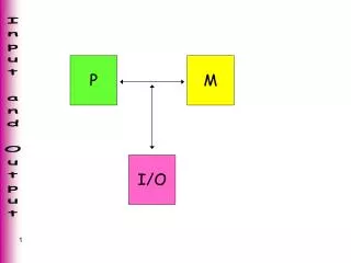
M68230 Parallel Interface/Timer • Used by M68000 to communicate with external devices. • Parallel data transfer. • Has three ports: • Port A, Port B, Port C. • Each port is 8-bits long. • Ports connect to devices. • Ports need to be initialized before used.
M68230 Interfacing M68k Memory CS* MAD (LED, Switches, Motor, 7-Segment, Keypad, etc.) M68230 CS* CS* Port A Device #1 Data Bus Port B Device #2 Port C Device #3
How M68230 connects to M68k D0-D7 D0-D7 PA0-PA7 DTACK* DTACK* PB0-PB7 R/W* R/W* CLK CLK PC0-PC7 RESET* RESET* A6-A23 MAD CS* (Register select pins) RS1-RS5 A1-A5 M68k M68230
Registers in M68230 • M68230 contains 23 registers. • Each of the registers have a unique address that refers to them. • To initialize ports, some registers need to be configured. • Port General Control Register. • Port X Control Register (A, B). • Port X Data Direction Register (A, B, C). • Port X Data Register (A, B, C).
PGCR • Port General Control Register. • Used to set the operation of Port A & Port B. • You only need to know (and use) Mode 0. • MOVE.B #$00,PGCR
PGCR= Mode Description $00 0 Unidirectional 8-bit transfer (Port A, Port B) $40 1 Unidirectional 16-bit transfer (Port A + Port B) $80 2 Bidirectional 8-bit transfer on Port B, bit I/O on Port A. $C0 3 Bidirectional 16-bit transfer (Port A + Port B) PGCR Settings
Port X Control Register • Used to set buffering of input/output on PXDR. • Three modes: • Mode 00. • Mode 01. • Mode 1X. • You only need to know (and use) mode 1X.
PXCR= Sub-mode Description $00 00 Double-buffered input $40 01 Double-buffered output $80 1X Bit I/O PXCR Settings
Port X Data Direction Register • Used to specify the direction of data transfer for each bit in the port. • Two states: • If PXDDR bit = 0, will be set as input. • If PXDDR bit = 1, will be set as output.
Port X Data Register • Contains the data sent/received to/from devices. • Each PXDR carries 8-bits of data. • There are three data registers in the M68230: PADR, PBDR, PCDR.
Port Initialization • To perform port initialization: • Assign the register addresses to a unique name. • PGCR must be set to #$00. • PXCR must be set to #$80. • Set PXDDR to input or output.
START ORG $XXXXXX PGCR EQU $A00001 PACR EQU $A0000D PBCR EQU $A0000F PADDR EQU $A00005 PBDDR EQU $A00007 PCDDR EQU $A00009 PADR EQU $A00011 PBDR EQU $A00013 PCDR EQU $A00019 MOVE.B #$00,PGCR MOVE.B #$80,PACR/PBCR MOVE.B #$XX,PADDR/PBDDR/PCDDR (DEPENDING ON THE H/W) Port Initialization Example Port Address PGCR $A00001 PACR $A0000D PBCR $A0000F PADDR $A00005 PBDDR $A00007 PCDDR $A00009 PADR $A00011 PBDR $A00013 PCDR $A00019
M68230 Interfacing • M68230 interfacing is similar to memory interfacing in last chapter. • Instead of interfacing memory, M68230 is interfaced. • A1-A5 is reserved for M68230, the rest used for decoder.
Example: Full Decoding • Interface M68230 with M68k so that its base address is $A50000.
Discussion • For M68230 interfacing, 5 lines are automatically reserved for M68230.
UDS/LDS (reserved) Step 1: Allocate Address Line A23 A22 A21 A20 A19 A18 A17 A16 A15 A14 A13 A12 A11 A10 A9 A8 A7 A6 A5 A4 A3 A2 A1 A0 X X X X X 5 lines allocated
UDS/LDS (reserved) Step 2: Set Base Address A23 A22 A21 A20 A19 A18 A17 A16 A15 A14 A13 A12 A11 A10 A9 A8 A7 A6 A5 A4 A3 A2 A1 A0 1 0 1 0 0 1 0 1 0 0 0 0 0 0 0 0 0 0 X X X X X A 5 0 0
Step 3: Find Lower Range A23 A22 A21 A20 A19 A18 A17 A16 A15 A14 A13 A12 A11 A10 A9 A8 A7 A6 A5 A4 A3 A2 A1 A0 1 0 1 0 0 1 0 1 0 0 0 0 0 0 0 0 0 0 0 0 0 0 0 0 A 5 0 0 0 0
Step 4: Find Upper Range A23 A22 A21 A20 A19 A18 A17 A16 A15 A14 A13 A12 A11 A10 A9 A8 A7 A6 A5 A4 A3 A2 A1 A0 1 0 1 0 0 1 0 1 0 0 0 0 0 0 0 0 0 0 1 1 1 1 1 1 A 5 0 0 3 F
NAND NAND A23 A16 A15 A8 A7 A6 AS* NAND Step 5: Design Decoder A23 A22 A21 A20 A19 A18 A17 A16 A15 A14 A13 A12 A11 A10 A9 A8 A7 A6 1 0 1 0 0 1 0 1 0 0 0 0 0 0 0 0 0 0 A 5 0 0 SELIO*
Memory Block Diagram $000000 unused $A50000 (Lower Range) Interfaced with M68k (M68230 I/O) $A5003F (Upper Range) unused $FFFFFF
Port Address PGCR $800001 PACR $800005 PBCR $800007 PADDR $800009 PBDDR $80000D PCDDR $80000F PADR $800011 PBDR $800013 PCDR $800019 Example 1: Set LED M68230 LED0 A set of LEDs are connected to Port B in M68230. Write a program that turns on LED3 and LED4, and turns off the rest. PB0 PB1 PB2 PB3 PB4 PB5 PB6 PB7 LED1 LED2 LED3 LED4 LED5 LED6 LED7
Discussion • Port B should be initialized before being used. • To turn on LED, the voltage at Port B bits should be high. • To turn off LED, the voltage at Port B should be low.
LED Operation B A A B LED 0 0 Zero biased (OFF) 0 1 Reverse biased (OFF) 1 0 Forward biased (ON) 1 1 Zero biased (OFF)
Solution START ORG $1000 PGCR EQU $800001 PBCR EQU $800007 PBDDR EQU $80000D PBDR EQU $800013 INIT MOVE.B #$00,PGCR MOVE.B #$80,PBCR MOVE.B #$FF,PBDDR ONLED MOVE.B #%00011000,PBDR END START
M68230 0 LED0 PB0 PB1 PB2 PB3 PB4 PB5 PB6 PB7 0 LED1 0 LED2 1 LED3 1 LED4 0 LED5 0 LED6 0 LED7 Example 1: Set LED
Example 2: Read Switches & Output to LED • A set of switches are connected to Port A, and a set of LEDs are connected to Port B in M68230. Write a program that reads the value in the switches and turns on the respective LEDs.
Switch Operation +5V Switch A OPEN 0 CLOSE 1 A R
Switch Operation +5V R Switch A A OPEN 1 CLOSE 0
Circuit Diagram +5V M68230 LED0 PA0 PB0 PA1 PB1 PA2 PB2 PA3 PB3 PA4 PB4 PA5 PB5 PA6 PB6 PA7 PB7 R LED1 R LED2 R LED3 R LED4 R LED5 R LED6 R LED7 R
Port Assignments Port Address PGCR $A00001 PACR $A0000D PBCR $A0000F PADDR $A00005 PBDDR $A00007 PCDDR $A00009 PADR $A00011 PBDR $A00013 PCDR $A00019
Discussion • Both Port A & B should be initialized before being used. • When the switch is OPEN, 5V is passed to M68230 (logic high). • When the switch is CLOSE, 0V is passed to M68230 (logic low).
Solution – Initialize Ports INIT MOVE.B #$00,PGCR MOVE.B #$80,PACR MOVE.B #$80,PBCR MOVE.B #$00,PADDR MOVE.B #$FF,PBDDR
Solution – Solve Problem LOOP MOVE.B PADR,D0 MOVE.B D0,PBDR BRA LOOP
Solution – Complete Program START ORG $1000 PGCR EQU $A00001 PACR EQU $A0000D PBCR EQU $A0000F PADDR EQU $A00005 PBDDR EQU $A00007 PADR EQU $A00011 PADR EQU $A00013 INIT MOVE.B #$00,PGCR MOVE.B #$80,PACR MOVE.B #$80,PBCR MOVE.B #$00,PADDR MOVE.B #$FF,PBDDR LOOP MOVE.B PADR,D0 MOVE.B D0,PBDR BRA LOOP END START
+5V M68230 0 LED0 PA0 PB0 PA1 PB1 PA2 PB2 PA3 PB3 PA4 PB4 PA5 PB5 PA6 PB6 PA7 PB7 R 1 LED1 R 1 LED2 R 0 LED3 R 1 LED4 R 1 LED5 R 0 LED6 R 1 LED7 R PADR D0 PBDR Sample Output
Consists of 7-LEDs arranged together. Can display numbers and characters. Each segment is marked with a letter (a to g). To display characters, need to turn on/off certain segments. Also has E (enable) pin to turn on/off 7-segment. 7-Segment
Interfacing 7-Segment with M68230 • To interface with M68230, each segment (a to g) is connected to a port in M68230. • The E signal must also be connected to a port to enable/disable the 7-segment.
7-Segment Types • There are two types of 7-segment displays: • Common cathode. • Common anode. • Each type differs in how they behave with certain inputs.
Input (from M68230) E Common Cathode 7-Segment E Input Output 0 0 OFF 0 1 ON 1 0 OFF 1 1 ON