Download
1 / 112
1.4k likes | 2.12k Views
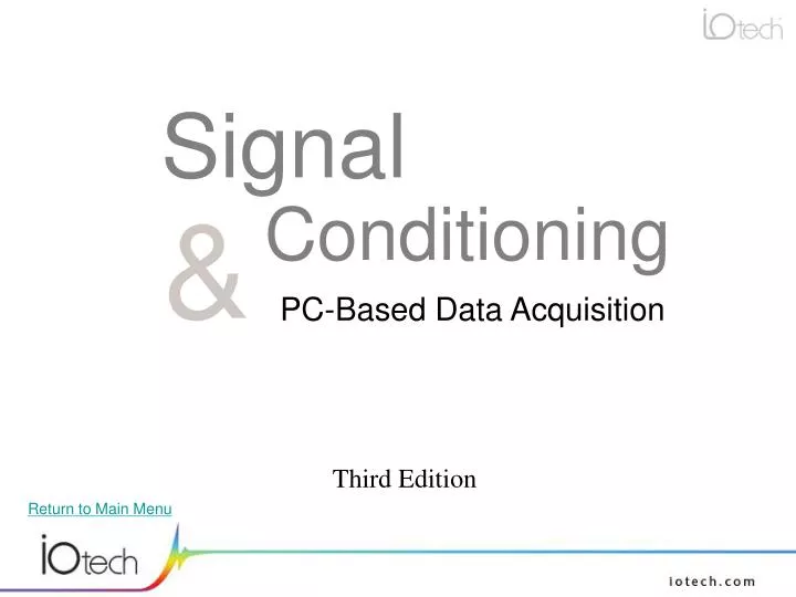
Signal Conditioning. &. PC-Based Data Acquisition. Third Edition. Main Menu. Chapter 1 Intro to Data Acquisition & Signal Conditioning Chapter 2 Analog to Digital Conversion Chapter 3 Multiplexing Chapter 4 Electrical Measurements Chapter 5 Fundamental Signal Conditioning

E N D
SignalConditioning & PC-Based Data Acquisition Third Edition
Main Menu Chapter 1 Intro to Data Acquisition & Signal Conditioning Chapter 2 Analog to Digital Conversion Chapter 3 Multiplexing Chapter 4 Electrical Measurements Chapter 5 Fundamental Signal Conditioning Chapter 6 Temperature Measurement Chapter 7 Strain Measurements Chapter 8 Vibration and Sound Chapter 9 Displacement and Position Sensing Chapter 10 Noise Reduction and Isolation Chapter 11 Digital and Pulse Train Signal Conditioning Chapter 12 Transducer Electronic Data Sheets
Introduction • Signals, Sensors, and Signal Conditioning • Data Acquisition Systems • PC-Based Data Acquisition Equipment
Analog to Digital (ADC) • ADC Types • Accuracy and Resolution • Noise Histograms • ADC Output Averaging • ADC Types • Accuracy and Resolution • Noise Histograms • ADC Output Averaging Chapter 1
Analog to Digital Conversion Analog-to-digital (A/D) converters are used to transform analog information, such as voltage signals or measurements of physical variables (for example, temperature, force, or shaft rotation) into a form suitable for digital handling, which might involve any of these operations: (1) processing by a computer or by logic circuits, including arithmetical operations, comparison, sorting, ordering, and code conversion, (2) storage on electronic media until ready for further handling, (3) display in numerical or graphical form on a computer, and (4) transmission Chapter 2
Analog to Digital Conversion • ADC Types • Successive Approximation Register • Voltage to Frequency • Integrating Dual Slope • Sigma-Delta Chapter 2
Analog to Digital Conversion • Successive-Approximation ADC • Usually associated with higher speed systems • Generally 12 and 16 bit • Inexpensive • Conversion process starts at Maximum range (MSB) and steps down through a defined sequence to the (LSB) until correct reading is found using a DAC and an analog comparator circuit. Figure 2.01 Chapter 2
Analog to Digital ConversionSuccessive approximation A / D example • Simple example of a 4 bit SAR A/D with 0 to 100 volt max range • 16 discreet steps (LSB 6.25) • For example: If the input voltage is 60V and the reference voltage is 100V, in the 1st clock cycle, 60V is compared to 50V (the reference, divided by two.) The voltage from the comparator is positive (or '1')(because 60V is greater than 50V). At this point the first binary digit (MSB) is set to a '1'. In the 2nd clock cycle the input voltage is compared to 75V (being halfway between 100 and 50V) because 60V is less than 75V, the comparator output is now negative (or '0'). The second binary digit is therefore set to a '0'. In the 3rd clock cycle, the input voltage is compared with 62.5V (halfway between 50V and 75V). The output of the comparator is negative or '0' (because 60V is less than 62.5V) so the third binary digit is set to a 0. The fourth clock cycle similarly results in the fourth digit being a '1' (60V is greater than 56.25V, the DAC output for '1001' followed by zeros). The result of this would be in the binary form 1001 Chapter 2
Analog to Digital Conversion • Sigma-Delta ADC • Usually associated with slower speed but higher accuracy • Over-sampling improves accuracy • Serial bit stream fed to LPF circuit • Effective sample rate output many times slower than A/D process loop • Noise reduction by spreading noise over larger sample freq using over-sampling and applying LPF and integration • Inherently linear • Resolution: 16 to 24 Bits Figure 2.04 Chapter 2
Sigma- Delta ADC Sigma-delta ADCs are far more complex than other ADC types. The oversampled analog signal goes through an integrator whose output drives a comparator (a 1-bit ADC) that, in turn, drives a 1-bit DAC in the feedback loop. Through a series of iterations, the integrator, comparator, DAC, and summing junction produce a serial bit stream that represents the oversampled input voltage. Once digitized, the oversampled signal goes through a digital filter to remove frequency components at or above the Nyquist frequency, which is one-half of the ADCs output-sampling rate (Ref. 4). A digital low-pass filter removes those high-frequency components, and a data decimator removes the oversampled data. In an ADC with 128X oversampling, the decimator will retain 1 bit for every 128 bits that it receives. The final output is a serial bit stream
Sigma-Delta ADC continued • Example: Let VIN=1.0V, VREF=2.5V. • The outputs from the comparator will be: 1, 0, 1, 1, 1, 0, 1, 1. • This means 6 of the 8 outputs have been a 1 • 6/8 = output is 75% of full-scale. • The allowed input range is -2.5 to +2.5 (+/-VREF) so the span is -2.5 to +2.5. • With a 1.0V input the input is 3.5V above the bottom of the 5.0V span or 70% of full-scale. • If we continue looping, the ones density of the above output stream will get closer and closer to 70%. • Example: After 27 clock tics from the comparator: (measured longer) • 101110110110111011011011101 = 19/27 = 70.3 % of full scale = • - 2.5 + 3.515 = 1.015 volts
Analog to Digital Conversion • Filter improves accuracy • 60 Hz Notch • High Resolution • Uses Oversampling • Input – High frequency • Output – Low Frequency • This technique can therefore be used effectively to increase the dynamic range of the ADC at the expense of overall output sampling rate and extra digital hardware • Sigma-Delta ADC with Digital Filter Figure 2.05 Chapter 2
Analog to Digital Conversion LETS Measure the same DC signal with: IOtech PersonalDaq/56 - Sigma-Delta ADC 22 – bit AND IOtech PersonalDaq/3000 – SAR ADC 16 - bit Chapter 2
Analog to Digital Conversion Table of ADC Attributes Figure 2.06 Chapter 2
Analog to Digital Conversion • A / D Resolution: • ADC resolution is the number of bits used to represent the analog input signal. To more accurately replicate the analog signal, you must increase the resolution. Using an ADC with higher resolution also reduces the quantization error (the unknown value between steps) • LSB (least significant bit) value = The smallest incremental voltage step of the A/D over a given range. (Not the smallest voltage step you can accurately measure!) • Calculate LSB value by converting the number of bits to the power of 2 and then dividing that number into the total span of the input voltage range of the data acquisition device. • 16 bit system with (+ / -) 10 volt input range = 20 volts / 65536 = 305 uV steps Chapter 2
Analog-to-Digital Conversion • ADC Accuracy: Accuracy is the degree of conformity of a measured or calculated quantity to its actual (true) value. • Errors in the A/D conversion process can affect Accuracy • Total system error = square root of the sum of each individual contributing error squared (root summed square) • Errors: Quantization error, Full Scale error, Offset error, Linearity, Missing digital codes Chapter 2
Analog-to-Digital Conversion • Factory Calibration – Recommended once every 12 months • Legacy hardware requires gain and offset adjusted via trim pots coefficients using precision calibration equipment. • Newer hardware often requires specialized software and equipment to digitally adjust gains and trim offsets.. • Customer receives new Calibration Certificate that indicating that the product meets the published specifications • Calibration Certificate often indicates equipment traceability. • System Calibration • Performed by end-user using software scaling. Does not change any factory calibration settings in the actual hardware device. • Calibrates system End-to-End to eliminate any offset errors including transducer interfacing and external signal conditioning Chapter 2
Analog to Digital Conversion • ADC Accuracy and Resolution • Quantization error – Part of the A/D conversion process • Quantization error results from an analog value that falls between digital steps. Worst case would be exactly half way between digital steps. (half LSB) • Quantization error shows up as noise on an FFT that is evenly distributed over the sample frequency range. Figure 2.07A Chapter 2
Chapter2Analog to Digital Conversion ADC Accuracy and Resolution • Gain Error - Part of the A/D conversion process • The same as Full Scale Error without the offset error • An A/D conversion error that is worst at the top end of a given range • Each conversion step has an equal ratio of gain error which adds up across the measurement range as more bits of the A/D are used. • Factory calibration corrects this using stored linear equation or look up table stored in the device by pivoting the conversion line on zero. • Expressed in LSB Figure 2.07B
Chapter2Analog to Digital Conversion • ADC Accuracy and Resolution • Linearity Error Part of the A/D conversion process • Some isolated portion along the conversion line becomes less accurate. • Should be 1 LSB or less • Some systems use • calibration points stored in • NVRAM lookup table. Figure 2.07C
Chapter2Analog to Digital Conversion • ADC Accuracy and Resolution • Missing Codes Part of the A/D • conversion process • Some A/D architectures • have missing binary conversion codes. • As the input voltage is swept over its • range, all output code combinations • should appear at the converter output. • Not as common of a problem • as technology has improved • Histogram would show zero samples at a • missing code location Figure 2.07D
Chapter2Analog to Digital Conversion • ADC Accuracy and Resolution • Offset Error • measured value has the same + / - offset from the actual value across the entire measurement range • Factory calibration • Offset is removed by aligning the negative most conversion code with zero and then adjusting for gain error by rotating the transfer function about the "new" zero point using a calibrated voltage source at full scale. The process is usually repeated. Figure 2.07E
Chapter2Analog to Digital Conversion • A / D Resolution: • While the A/D converters used on most 16-bit boards are extremely accurate, other circuitry is usually not. 16-bit accuracy in analog circuits is very hard to achieve. Gains greater than one, high sampling rates, and input signals that change rapidly from zero volts to full-scale all tend to reduce the accuracy of the board’s analog circuitry. In handling real-world signals, analog circuitry sometimes becomes the limiting element on overall accuracy. • ENOB (Effective Number of Bits) test is a common way to scrutinize a data acquisition system to determine the total accuracy that a system will have under realistic user conditions including specified interface cabling. • The results of this test might state something like – This 16 bit Daq system has a Total Accuracy of 14.5 bits when used in my exact application setup
Chapter2Analog to Digital Conversion • ENOB: • Effective Number of Bits - FFT display • Typical distribution of samples from an ENOB test. A software utility could be developed to perform this test • Software can calcluate SINAD with this data and then compute ENOB Figure 2.08
A / D Resolution ENOB test example: • Install or plug the data acquisition system to be tested into a computer. Because tests involve the • entire board, not just IC-level subsystems purchased from other vendors, everything that can affect • performance is covered, including configuration of the subsystems, how they are interconnected and • operated. • 2. Connect a test signal to one of the modules analog input channels. This signal should come from a precision generator, accurate to at least .001%, and providing a very low noise, very low distortion • sine wave. Any noise or distortion detected after the signal is acquired is contributed by the board or • module itself. Set the test signal’s voltage level to within 1 dB of the maximum input range of the • board. Set the frequency to a known value, typically 1kHz, providing a reference point when comparing different modules. • 3. Ground a second input channel on the module. This represents the lowest signal level the module will see. • 4. Make connections to the module using the cables and screw terminal panels recommended by the • manufacturer. The tests occur under real-world conditions, in the environment that you would run the system under normal test conditions. • 5. Run a testing program that represents the most demanding input conditions the module is designed to see: • a. Operate the Data Acquisition system at full rated sample speed. • b. Alternate between sampling the test signal and the grounded input. • c. Going rapidly from no input to full-scale input at full rated throughput exposes slewing, bandwidth, and distortion errors, and fully exercises the analog input circuitry on the module. • d. Capture 1024 samples on each input channel. A large number of samples is required so the sophisticated FFT algorithm in the test program can compute ENOB with statistical accuracy. • e. Calculate and display ENOB – the number of bits of effective accuracy. A Programming interface software package such as Dasylab or Labview could be used to perfrom the FFT and calculate and display ENOB. • The ratio of good samples to bad samples translates to the number of good bits versus bad bits to calculate the Effective Number of Bits.
Chapter2Analog to Digital Conversion • ENOB example: • From the acquired FFT of 1024 points of the test signal . • ‘A-signal’ represents the RMS value of the peak of the fundamental frequency. • ‘A-noise’ is the RMS value of each of the remaining points within half of the sample frequency range. • As en example, a tested Data Acquisition Board has a SINAD of 64 dB when measuring a 1 MHz sinusoid at full scale range. Thus, effective number of bits for this signal is:
Chapter2Analog to Digital Conversion • ENOB: • Effective Number of Bits • Histogram Display • A histogram is the graphical version of a table which shows what proportion of cases fall into each of several or many specified categories • Typical distribution of samples from an ENOB test on a histogram display. • This histogram illustrates how 12-bit ADC samples in a set were distributed among the various codes for a 2.5-V measurement in a range of 10 volts. Most codes ended up at 1024 (2.5v) but others fell under a Gaussian distribution due to white noise content Figure 2.08
Chapter2 • Real Histogram test from Labview • Troubleshooting missing code problem
The ENOB Test ADC MUX PGA SSH Amp Cross talk FFT Test Results Slewing Harmonic Distortion Analog Circuits ADC Accuracy Noise Pickup Channel Cross Talk Nonlinearities Channel Offset Chapter2Analog to Digital Conversion
Chapter2Analog to Digital Conversion ADC Output Averaging • Improved Accuracy • More Stable Readings • Gaussian Distribution
Chapter2Analog to Digital Conversion ADC Output Averaging • SOURCES OF NOISE • - The Data Acquistion System itself. • - SIGNAL WIRES are subject to EMI ((electromagnetic interference) (60Hz noise) and RFI (Radio frequency interference) (computer noise), both of which can induce noise on the wires carrying the transducer signal to the A/D board. • - SENSOR NOISE - Sometimes it is necessary to electrically isolate the sensor from the measured medium TYPES of Noise - Periodic noise: (such as sine waves, especially 50 or 60 Hz noise) - Random noise: broad range of frequencies of random amplitude – (Gaussian noise) (white noise)
Chapter2Analog to Digital Conversion ADC Output Averaging Averaging Types Software running average: Reduces RANDOM noise using asmoothing factor controlled by you through the software can be increased or decreased to specify the number of actual waveform data points or samples that the moving average algorithm will use. A waveform can be thought of as a long string or collection of data points. The algorithm accomplishes a moving average by taking two or more of these data points from the acquired waveform, adding them, dividing their sum by the total number of data points added, replacing the first data point of the waveform with the average just computed, and repeating the steps with the second, third, and so on data points until the end of the data is reached. The result is a generated waveform consisting of the averaged data and having the same number of points as the original waveform. - Noise is typically reduced by the square root of the number of averaged samples. Remember -The sample rate has to be increased behind the scenes to accommodate this !!!! You cannot exceed the highest sample rate of the system
Chapter2Analog to Digital Conversion ADC Output Averaging • Averaging Types • Line cycle averaging • - A mode that is typically enabled in software which adjusts the selected sample rate of the data acquisition system to fit the number of samples taken perfectly within one cycle of either a 50 Hz or 60 Hz waveform (evenly spaced). • - synchronizes a series of readings with the power line frequency and averages the series—nulls out the effect of most AC line noise on the signals.
Chapter2Analog to Digital Conversion ADC Output Averaging • Averaging Types • Over Sampling (per channel) • - Forces a multiplexed data acquisition system to sit on a designated channel for X number of samples and then averages those samples together to create the measured value. • - Acts like a LPF because it will average out spikes or noise that would show up during high speed mux transitions. • - Increases settling time on each channel so that signal can stabilize. • - Very common with Sigma Delta ADC systems to increase accuracy by reducing noise. These systems are usually slower scanning systems that are designed for higher accuracy. Excellent for Thermocouples and slow changing voltage signals such as pressure sensors.
Chapter2Analog to Digital Conversion ADC Output Averaging • IOtech PersonalDaq/3000 – Software Running Average Example
Chapter2Analog to Digital Conversion Return To Main Menu Continue to Next Chapter
Chapter3Multiplexing and Sampling Theory • The Economy of Multiplexing • Fundamental Concepts
Chapter3Multiplexing and Sampling Theory • Multiplexers • Scans Numerous Channels • Uses Single ADC • Reduces Cost • Reduces Acquisition Rate • Will probably disappear in future due • due to technology improvements and • low cost A/D. You will have an A/D per channel Figure 3.01
Chapter3Multiplexing and Sampling Theory • Mux With Selectable Gain • Selects Channel • Sets Gain • All Channels Scanned at Same Rate • Typical: 512 Scan/Gain combinations and each channel can have different gain Figure 3.03
Chapter3Multiplexing and Sampling Theory • Sample and Hold • Time Skew Problem • Sample & Hold Circuit • Works With Multiplexer • Instrumentation Amp • Low-Pass Filter • Sample & Hold Circuit • Low Impedance Amps Figure 3.05
Chapter3Multiplexing and Sampling Theory • Inadequate Nyquist sample rate • Nyquist = The Sampling Theorem states that a signal can be exactly reproduced if it is sampled at a frequency F, where F is greater than twice the maximum frequency in the signal. (usually 2.56 x) • This is important when selecting a data acquisition system for applications that involve waveform capture and dynamic signals. • Aliasing is a false waveform that appears in the data due to connecting too few sample points. Figure 3.06
Chapter3Multiplexing and Sampling Theory • Acceptable NyquistSampling Rate • Original Signal Preserved after being digitized by A/D • IOtech PersonalDaq/3000 Aliasing live example Figure 3.07
Chapter3Multiplexing and Sampling Theory • Mux Settling Time in multiplexed A/D systems • Source Impedance –The output impedance of the transducer or circuit you • are connecting needs to have low impedance when interfacing to a DAQ system that • multiplexed without buffering. - A good rule of thumb is to stay below 1 K ohms - • The multiplexer needs to discharge a small electrical build up charge back through • the signal connection - Otherwise errors result in the measurement - • Systems with fast channel to channel scan times do not have enough settling time per channel to allow • for proper mux charge bleed off. Some systems allow you to increase the settling time per channel which • will slow down the overall scan rate of the system (trade off) • Stray Capacitance – Likewise, connecting large external capacitance is not recommended • Frequency Range – High external R/C will also reduce frequency response with the mux • Buffer Amplifier – Most manufacturers of these types of DAQ systems will have a tech tip • on how to add your own external buffer circuit between your high R / C device and the • un-buffered DAQ system or have an add on module to add to the system with buffering
Chapter3Multiplexing and Sampling Theory Return To Main Menu Continue to Next Chapter
Chapter 4Electrical Measurements • Valid Measurements • DC Voltage • AC Voltage • Current • Resistance • Wheatstone Bridges • Single-Ended & Differential Measurements • Kelvin Connections
Chapter 4Electrical Measurements • Making Valid Measurements • Calibration – Factory and possible system cal in the field • Shielding – Twisted shielded pair with the shield tied to ground at only one end • Filtering – LPF if available set to just above the frequency of interest • Grounding – slight ground differences between unit under test and DAQ system are a setup for ground loops.
Chapter 4Electrical Measurements • DC Voltage • Instrument Level – most DAQ systems have max of + / - 10 v on their base voltage inputs. • Usually the mfg will offer additional add on signal conditioning that converts signal types out side of this range and then feeds them into the base + / - 10 volt inputs of the system. • Gain ranges can be set per channels from + / - 10 down to + / - 156mv • High Voltage – Either voltage divider (be careful of high resistance on input) • Or use a designated converter option or 5B module. • Low Voltage – Remember ENOB and noise follow issues when trying to measure millivolt level signals. Usually the highest gain range on a base DAQ system is not high enough gain for transducers like strain gages and thermocouples which output millivolts • In this case a special high gain module needs to be used or 5B modules. • In some cases 22 bit Sigma Delta A/D systems can make these measurement if you are careful • Range Switching – Most DAQ systems cannot change the range during a measurement.
Chapter 4Electrical Measurements • AC Voltage • Low Voltage • pay attention to input channel range and p-p of your AC signal to measure • Most DAQ systems will capture the actual waveform and will not report RMS • 5B modules can report RMS directly • Some advanced software can convert to RMS on PC (Dasylab, Labivew) • High Voltage • Divider circuit with Diff Buffers • IOtech offers high voltage converter cards Figure 4.01
Chapter 4Electrical Measurements • Shunt Resistor Current Measurement • 4-20 mA Current Loop Figure 4.06
Chapter 4Electrical Measurements • Current Measurements • 4-20ma current loops – A common instrumentation signal that uses a changing current value to represent transducer or process values. A DAQ system can easily decode this by placing a 250 Ohm resistor across the HIGH and LOW inputs of a base differential voltage input. The DAQ system will read the voltage across the resistor and report a voltage between 1 volt and 5 volt which is directly proportional to 4 – 20 ma. • -Differential inputs should be used so as to not accidentally tie the DAQ ground to a non ground part of the 4-20ma loop. • Common Mode Limits • - If using non isolated inputs you must make sure that the common mode voltage to system ground does not exceed the specification of the DAQ system. This involves careful placement of the shunt resitor. • - Isolated inputs such as 5B modules would eliminate this concern