Download
1 / 34
350 likes | 457 Views
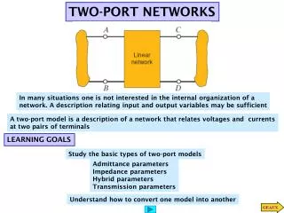
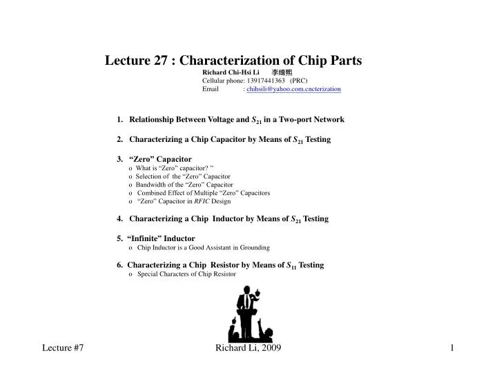
Lecture 27 : Characterization of Chip Parts Richard Chi-Hsi Li 李缉熙 Cellular phone: 13917441363 (PRC) Email : chihsili@yahoo.com.cncterization. 1. Relationship Between Voltage and S 21 in a Two-port Network 2. Characterizing a Chip Capacitor by Means of S 21 Testing

E N D
Lecture 27 : Characterization of Chip Parts Richard Chi-Hsi Li李缉熙 Cellular phone: 13917441363 (PRC) Email : chihsili@yahoo.com.cncterization • 1. Relationship Between Voltage and S21in a Two-port Network • 2. Characterizing a Chip Capacitor by Means of S21 Testing • 3. “Zero” Capacitor • o What is “Zero” capacitor?” • o Selection of the “Zero” Capacitor • o Bandwidth of the “Zero” Capacitor • o Combined Effect of Multiple “Zero” Capacitors • o “Zero” Capacitor in RFIC Design • 4. Characterizing a Chip Inductor by Means of S21 Testing • 5. “Infinite” Inductor • o Chip Inductor is a Good Assistant in Grounding • 6. Characterizing a Chip Resistor by Means of S11 Testing • o Special Characters of Chip Resistor Richard Li, 2009
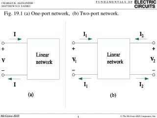
Relationship Between Voltage and of S21 in a Two-port Network • [Ralph S. Carson, “High-Frequency Amplifiers,” (Book) , John Wiley & Sons, Inc., 1975.] Port 1 Port 2 Two-port Network R01 R02 v1 v2 E2 E1 Figure 1 Source and load parameters in a two-port network E2 = 0, Ω, Richard Li, 2009
Network Analyzer (S21 testing) Port 2 Port 1 50 Ω 50 Ω Figure 2 S21 testing for a chip capacitor. DTU ChipC GND 2. Characterizing a Chip Capacitor by Means of S21 Testing Richard Li, 2009
Port 1 Port 2 LS 50 ohm v1 v2 50 ohm C E1 RS • Figure 3 Replacement of “Two port Network” in Figure 2 • by chip capacitor’s equivalent model . Richard Li, 2009
S21, dB 40 30 20 10 0 -10 -20 -30 -40 Cspecified = 15 pF S21,SRF = -45.1dB SRF = 1.394 GHz -50 -60 1.0 1.1 1.2 1.3 1.4 1.5 1.6 1.7 1.8 1.9 2.0 2.1 2.2 f , GHz • Figure 4 S21Frequency response of chip capacitor C= Cspecified =15 pF with • test setup as shown in Figure 14A.1. 15 pF Richard Li, 2009
fSRF , MHz 10000 • fSRF= 5400 / C1/2 • (MHz) (pF) • 1. 8 pF < Cspecified < 18000 pF • Size : 30x60 & 50x80 mils2 1000 Inductive Application Region Capacitive Application Region 100 10 1 10 100 1000 10000 100000 1000000 10000000 Cspecified, pF • Figure 5 Plot of the self-resonant frequency fSRFvs specified value of chip capacitor Cspecified, • extrated from testing of MuRata chip capacitors. Richard Li, 2009
Table 1 Some important SRFC (Self Resonant Frequency) values of chip capacitors • SRFCValue of chip capacitor, • (MHz) (pF) • 40 18,000 • 150 1,296 • 450 144 • 500 117 • 800 46 • 900 36 • 1,000 29 • 1,500 13 • 2,400 5.1 • 5,400 1.0 Richard Li, 2009
LS , nH 1 • LS = 0.86 nH • 1. 8 pF < Cspecified < 18000 pF • Size : 30x60 & 50x80 mils2 0.1 0.01 1 10 100 1000 10000 100000 1000000 10000000 Cspecified, pF • Figure 6 Plot of in-series parasitic inductance LS vs specified capacitance Cspecified, • extracted from testing of MuRata chip capacitors. Richard Li, 2009
RS , Ω 1 • RS = 0.08 to 0.52 Ω • 1. 8 pF < Cspecified < 18000 pF • Size : 30x60 & 50x80 mils 0.1 0.01 1 10 100 1000 10000 100000 1000000 10000000 Cspecified, pF Figure 7 Plot of in-series resistance RS vs specified capacitance Cspecified, extrated from testing of MuRata chip capacitors. Richard Li, 2009
Vcc Bias AC Bypass Capacitor AC Bypass Capacitor GND L1 GND Out R1 In DC Blocking Capacitor Q1 DC Blocking Capacitor GND Figure 8 “Zero” capacitor functions as a bypass or a blocking capacitor 3. “Zero” Capacitor o What is a “Zero” Capacitor? “Zero” Capacitor = AC Bypass capacitor = DC Blocking capacitor Richard Li, 2009
C L C r (a) An actual chip capacitor Figure 9 An actual chip capacitor and its equivalent o Selection of the “Zero” Capacitor Theory Chip “zero” capacitor (b) Equivalent of an actual capacitor For MuRata capacitors Cspecified = 0.5 pF to 18000 pF. for both sizes W x L = 50 x 80 mils and 30 x 40 mils where SRFc = Self resonant frequency in MHz, Cspecified= Specified capacitance by the manufacturer in pF. Richard Li, 2009
“Zero” capacitor Vdd G P PC B Figure 10 RF or AC grounded by a “zero” capacitor on a PCB (Printed Circuit Board). • Top metallic area; P : Point to be grounded; • Bottom metallic area; G : Reference ground point.. • Conductive via from top to bottom; • “Zero” capacitor * “Zero” capacitor on PCB in narrow band case Richard Li, 2009
“Zero” capacitors Vdd G P PC B • Figure 11 RF or AC grounded by more than one “zero” capacitor on a PCB • (Printed Circuit Board). • Top metallic area; P : Point to be grounded; • Bottom metallic area; G : Well-grounded point. • Conductive via from top to bottom; • “Zero” capacitor * “Zero” capacitor on PCB in wide band or multi-band case Richard Li, 2009
or Vdd Vdd RF block RF block (a) 1 or 2 “Zero” capacitors for a RF block Vdd2 Vdd1 RF system Vdd3 (b) More “Zero” capacitors for a RF block • Top metallic area; P : Point to be grounded; • Bottom metallic area; G : Reference ground point.. • Conductive via from top to bottom; • “Zero” capacitor Figure 12 Number difference of “zero” capacitor in a RF system and in a RF block * Number of “zero” Capacitors in a RF system are much more than in a RF block Richard Li, 2009
Figure 13 “Zero” capacitor works in the RF/AC grounding for a IC die Bond wire Pad Top metallic area Bottom metallic area IC die Runner in IC die Runner on IC die Soldering pad on PCB Conductive via from top to bottom Chip “zero” Capacitor Ground ring of RF block RF Block IC die Chip “zero” capacitor PCB (Printed Circuit Board) * “Zero” Capacitors in RFIC Richard Li, 2009
Network Analyzer (S21 testing) Port 1 Port 2 DUT 50 Ω 50 Ω ChipC GND Figure 14 S21 testing for a chip capacitor. o Bandwidth of the “Zero” Capacitor Richard Li, 2009
S21, dB 40 30 15 pF 20 BW =1.600 - 1.230 = 0.370 GHz 10 0 -10 BW =1.475 - 1.310 = 0.165 GHz -20 -30 BW =1.422 - 1.352 = 0.070 GHz -40 Cspecified = 15 pF S21,SRF = -45.1dB SRF = 1.394 GHz -50 -60 1.0 1.1 1.2 1.3 1.4 1.5 1.6 1.7 1.8 1.9 2.0 2.1 2.2 f , GHz • Figure 15 S21 frequency response of a chip capacitor tested • with setup as shown in Figure 14.11 Richard Li, 2009
S21, dB 40 30 20 10 BW =1.560 - 1.310 = 0.250 GHz 0 -10 -20 -30 -40 Cspecified = 15 pF S21,SRF = -45.1 dB SRF = 1.394 GHz Cspecified = 13 pF S21,SRF = -42.6 dB SRF = 1.456 GHz -50 -60 1.0 1.1 1.2 1.3 1.4 1.5 1.6 1.7 1.8 1.9 2.0 2.1 2.2 f , GHz • Figure 16 Frequency bandwidth 250 MHz =1.560 -1.310 GHz is covered by a “zero” capacitor • combined by two capacitors C= 15 pF and C= 13 pF connected together in parallel. 15 pF 13 pF Richard Li, 2009
Figure 17 Modified equivalent model of “zero” chip capacitor by adding of soldering pads and runners for RF modules Runner on IC die “Zero” chip capacitor Soldering pad on PCB * Combined Effect of Multiple “Zero” Capacitors An interesting question is then raised: Does a resultant SRF due to the combination of all the individual “zero” capacitors exist, superseding the SRFs of the individual “zero” capacitors, since these “zero” capacitors are connected between the positive terminal of DC power supply or DC bias and a real grounded point, GND, in parallel? According to empirical experimentation, a resultant SRF combined by individual “zero” capacitors may appear while the behavior of the individual “zero” capacitors is unchanged. The resultant SRF is usually located outside of the expected bandwidth. Richard Li, 2009
Network Analyzer (S21 testing) Port 2 Port 1 50 Ω 50 Ω Figure 18 S21 testing for a chip inductor. DTU ChipL GND 4. Characterizing a Chip Inductor by Means of S21 Testing Richard Li, 2009
Port 1 RP Port 2 L CP 50Ω v1 v2 50 Ω E1 Two-port network • Figure 19 Replacement of “Two port Network” in Figure 14A.3 by • chip inductor’s equivalent model Richard Li, 2009
S21, dB 40 62nH 30 20 10 0 -10 -20 -30 -40 L = Lspecified S21,SRF = - 46.7 dB SRF = 1.57 GHz -50 -60 1.0 1.1 1.2 1.3 1.4 1.5 1.6 1.7 1.8 1.9 2.0 2.1 2.2 f , GHz • Figure 20 S21Frequency response of chip inductor L= 62 nH • with test setup as shown in Figure 14A.2. Richard Li, 2009
Table 2 Some SRFL (Self Resonant Frequency) values of chip inductors • SRFLValue of chip inductor, • (MHz) (nH) • 210 1,800 • 300 884 • 450 393 • 500 318 • 800 124 • 900 98 • 1,000 79.6 • 1,500 35.4 • 2,400 13.8 • 5,400 2.7 Richard Li, 2009
fSRF , MHz 10000 • fSRF = 8920 / L1/2 • (MHz) (nH) • 22 nH < Lspecified,< 1800 nH Capacitive Application Region 1000 Inductive Application Region 100 10 100 1000 10000 Lspecified,, nH Figure 21 Plot of the self-resonant frequency fSRF vs specified value of chip inductor Lspecified, extracted from testing of MuRata chip inductors. Richard Li, 2009
CP , pF 10 • CP = 0.2 pF • 22 nH < Lspecified < 1800 nH 1 0.1 10 100 1000 10000 Lspecified, nH Figure 22 Plot of in-parallel capacitance CP vs specified inductance Lspecified, extracted from testing of MuRata chip inductors. Richard Li, 2009
RP , Ω 1000000 • RP = 2580 x L1/2 • (Ω) (nH) • 22 nH < Lspecified< 1800 nH 100000 10000 1000 10 100 1000 10000 Lspecified, nH Figure 23 Plot of in-parallel resistance RP vs specified inductance Lspecified, extrated from testing of MuRata chip inductors. Richard Li, 2009
C C L r (a) An actual inductor (b) Equivalent of an actual inductor Figure 24 An actual inductor and its equivalent o Chip Inductor is a Good Assistant Theory Chip “Infinite” inductor For MuRata inductors Lspecified = 22 nH to 1800 nH. where SRFL = Self resonant frequency in MHz, Lspecified= Specified capacitance by the manufacturer in nH. Richard Li, 2009
“Infinite” inductor Vdd or Vcc Po P GND “Zero” capacitor PC B Figure 25 RF or AC grounded by a “zero” capacitor with assistance of an “infinite” inductor on a PCB. • Top metallic area; P : Point to be grounded; • Bottom metallic area; GND : Reference grounded point. • Conductive via from top to bottom; • “Zero” capacitor • “Infinite” inductor Richard Li, 2009
Figure 26 “Zero” capacitor is connected between the P+ guard ring in IC die • and the ground frame on PCB Bond wire Pad Top metallic area Bottom metallic area IC die Runner in IC die Runner on IC die Soldering pad on PCB Conductive via from top to bottom Chip “zero” Capacitor Ground ring of RF block RF Block IC die Chip “zero” capacitor PCB (Printed Circuit Board) o “Zero” Capacitor in RFIC Design Richard Li, 2009
(b) “Zero” capacitor grounding for a RF module or for a RF block built by discrete parts (a) “Zero” capacitor grounding for a RFIC die Figure 27 Difference of “Zero” capacitors RF/AC grounding for a IC die and for a RF module or a RF block module Bond wire Pad IC die Runner in IC die Runner on IC die Soldering pad on PCB Chip “zero” Capacitor • A shout runner in IC die from the ground • ring die to a tiny pad, • A tiny bond pad in IC die, • A bond wire in the air between the tiny pad • in IC die and the bonding pad on PCB, • A bonding pad on PCB • A runner on PCB from the bonding pad on • PCB to the soldering pad on PCB, • Soldering pad on PCB, • A chip “zero” capacitor, • Soldering pad on PCB, • A runner on PCB between the chip “zero” • capacitor and the ground frame on PCB. • A runner on PCB from the point to be • grounded to a soldering pad, • Soldering pad on PCB, • A chip “zero” capacitor, • Soldering pad on PCB, • A runner on PCB between the chip “zero” • capacitor and the ground frame on PCB. Richard Li, 2009
Network Analyzer (S11 testing) Port 2 Port 1 DTU ChipR 50 Ω Figure 28 S11 testing for a chip resistor. 5. Characterizing a Chip Resistor by Means of S11 Testing Richard Li, 2009
Port 1 ZS 50 Ω (or) RP CP LP E1 One-port Network Figure 29 Single-port S-parameter measurement of a chip capacitor Richard Li, 2009
RP , Ω 1000000 • RP = Rspecified ,if f < 100 MHz 100000 10000 1000 100 10 f < 100 MHz f = 500 MHz f = 1000 MHz f = 1500 MHz f = 2000 MHz 1 10 100 1000 10000 100000 Rspecified, Ω • Figure 30 Plot of in parallel resistance RP vs. specified resistance Rspecified, • extrated from testing of MuRata chip resistors. Richard Li, 2009
CP , pF 10 • CP= 0.65 to 0.90 pF , • if 150 Ω < Rspecified <51000 Ω 1.0 0.1 10 100 1000 10000 100000 Rspecified, Ω f = 1500 MHz f = 2000 MHz f < 100 MHz f = 500 MHz f = 1000 MHz Figure 31 Plot of in-parallel capacitance CP vs specified resistance Rspecified, extrated from testing of MuRata chip resistors. Richard Li, 2009