Download
1 / 49
560 likes | 970 Views
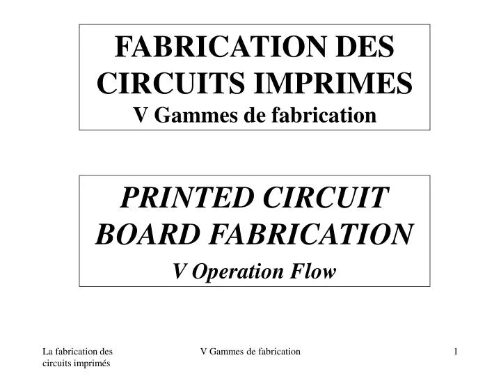
FABRICATION DES CIRCUITS IMPRIMES V Gammes de fabrication. PRINTED CIRCUIT BOARD FABRICATION V Operation Flow.

E N D
FABRICATION DES CIRCUITS IMPRIMESV Gammes de fabrication PRINTED CIRCUIT BOARD FABRICATION V Operation Flow V Gammes de fabrication
1 Circuit simple face Single-sided board2 Circuit double face Double-sided board3 Circuit multicouches Multilayer board4 Circuit souple Flexible board5 Circuit Flexo-rigide Flex-rigid circuit Gammes de FabricationOperation Flows V Gammes de fabrication
1 Circuits Simple FacePrincipe de base Single-Sided Board Overview V Gammes de fabrication
Sommaire Outlook - Diagramme Flow-chart - Vue côté soudure Solder-side view - Matière de base Base material - Transfert image Imaging - Gravure Etching - Élimination de la résine photosensible Stripping - Perçage Drilling V Gammes de fabrication
Sommaire Outline - Vernis épargne-soudure Solder mask - Traitement du cuivre Copper-finishing - Marquage Screen-printing - Détourage Routing - Test électrique Electrical test - Contrôle Inspection - Expédition Shipping V Gammes de fabrication
Diagramme Flow chart Découpe des ébauches Panel-cutting Vernis épargne Solder mask Contrôles-tests Tests- Final Inspection Transfert image Imaging Finitions Finishing Expédition Shipping Gravure Etching Marquage Screen printing Perçage Drilling Détourage Routing V Gammes de fabrication
Section view Plan de coupe (circuit nu) (bare board) Vue côté soudure Solder side view V Gammes de fabrication
Matière de base Base Material Cuivre 9 à 105 µm 9 to 105 µm copper Stratifié 1 à 3,2 mm ( FR2, FR3, FR4, CEM ) 1 to 3.2 mm laminate ( FR2, FR3, FR4, CEM ) V Gammes de fabrication
Transfert image Imaging Etch mask : ink or photoresist Réserve de gravure : encre ou résine photosensible V Gammes de fabrication
Gravure Etching Pulvérisation de l ’agent de gravure etchant spray V Gammes de fabrication
Élimination de la réserve de gravure Stripping Pulvérisation de solvant stripper spray V Gammes de fabrication
Perçage / Poinçonnage Drilling / Punching Foret ou outil de presse Drill or punching tool V Gammes de fabrication
Vernis épargne-soudureSolder mask Dépôt de vernis par sérigraphie Screen-deposited solder resist V Gammes de fabrication
Traitement du cuivre Copper finishing étamage / passivation tinning / passivation V Gammes de fabrication
Marquage Screen printing Sérigraphie du motif screen-printing R 69 Côté composants component layer V Gammes de fabrication
Fermé ? Short ? Test électrique Electrical test Ouvert ? Open ? V Gammes de fabrication
Contrôle FinalInspection V Gammes de fabrication
Expédition Shipping V Gammes de fabrication
2 Circuits Double Faces Trous MétallisésPrincipe de base Double-Sided Plated-Through Hole Boards Overview V Gammes de fabrication
Sommaire Outlook - diagramme Flow-chart - Vue côté composant Component side view - Matière de base Base material - Perçage Drilling - 1ère métallisation 1st plating - Transfert image Imaging - 2ème métallisation 2nd plating - Élimination de la résine Photoresist stripping V Gammes de fabrication
Sommaire Outline -Gravure Etching -élimination SnPB SnPb stripping -Vernis épargne-soudure Solder mask -Étamage H.A.L. H.A.L. tinning -Marquage Screen printing -Détourage Routing -Test électrique Electrical test -Contrôle Inspection -Expédition Shipping V Gammes de fabrication
Diagramme Flow-chart Découpe des ébauches Panel-cutting Métallisation Plating Perçage Drilling Élimination résine Stripping Métallisation Plating Gravure Etching Transfert image Imaging V Gammes de fabrication
Diagramme Flow-chart Marquage Screen printing Élimination Sn Pb SnPb-stripping Détourage Routing Vernis épargne Solder mask Contrôle-tests Inspection-tests Finition Finishing Expédition Shipping V Gammes de fabrication
Section view Plan de coupe (circuit nu) (bare board) Vue côté composantsComponent-side View V Gammes de fabrication
Matière de baseBase material Cuivre 9 à 105 µm 9 to 105 µm copper Stratifié 1 à 3,2 mm ( FR4, CEM3 ) 1 to 3.2 mm laminate (FR4, CEM3 ) V Gammes de fabrication
Perçage Drilling foret drill bit V Gammes de fabrication
Première métallisationFirst plating Cuivre chimique + renfort électrolytique electroless copper + electrolytic copper plating V Gammes de fabrication
Transfert imageImaging Réserve de métallisation (résine photosensible) Plating mask (photoresist) V Gammes de fabrication
Seconde métallisationSecond plating Copper plating (25µm) + alloy plating (5µm) Dépôt électrolytique de cuivre (25µm) et alliage (5µm) V Gammes de fabrication
Elimination de la réserve Stripping Pulvérisation de solvant Stripper spray V Gammes de fabrication
GravureEtching Pulvérisation de l ’agent de gravure Etchant spray V Gammes de fabrication
Elimination du dépôt SnPbStipping Pulvérisation de solvant Stripper spray V Gammes de fabrication
Vernis épargne-soudureSolder mask Dépôt de vernis par sérigraphie Screen-deposited solder resist V Gammes de fabrication
Etamage H.A.L.H.A.L. tinning Dépôt SnPb par bain et nivelage à l ’air chaud Tin bath deposit and hot air levelling V Gammes de fabrication
R 69 Marquage Screen printing Sérigraphie du motif screen printing Côté composants component layer V Gammes de fabrication
Fermé ? Short ? Test électrique Electrical test Ouvert ? Open ? V Gammes de fabrication
Contrôle Final Inspection V Gammes de fabrication
Expédition Shipping V Gammes de fabrication
3 Circuits MulticouchesPrincipe de base Multilayer PCBs Overview V Gammes de fabrication
Sommaire Outline - Diagramme Flow chart - Poinçonnage Punching - Empilage Stacking - Pressage Lamination - Paramètres Parameters V Gammes de fabrication
Diagramme Flow-chart Découpe des ébauches Panel-cutting Test optique Optical test Préimprégnés / cuivres Prepregs / copper foils Trous pilotes Locating holes Préparation de surface surface preparation Empilage / pressage Stacking / lamination Transfert image Imaging Trous pilote / détourage Locating holes / routing Gravure Etching Gamme DFTM DSPTH flow V Gammes de fabrication
Poinçonnage des trous de registrationPunching of tooling holes Détrompeur Center off hole Trou de registration Tooling hole Pion de registration Dowel pins V Gammes de fabrication
Empilage Stacking Moule de pressage Coussin de pressage Tôle de séparation Démoulant Construction MC ML construction Realise film Separator plate Press padding Press form V Gammes de fabrication
Pressage Lamination Presse hydraulique ou autoclave Hydraulic or autoclave press T° T° P V Gammes de fabrication
Paramètres de pressagePressing parameters Pressage sous vide Vacuum chamber press Pression (bar) Pressure(bar) Température (°C) Temperature (°C) 180 15 120 10 60 5 90 Temps (mn) Time (mn) 30 60 V Gammes de fabrication
4 Circuits SouplesPrincipe de base Flexible PCBs Overview V Gammes de fabrication
Diagramme Flow-chart Découpe des ébauches Panel-cutting Isolants adhésifs Adhesive coverlay Trous pilotes Locating holes Empilage / pressage Stacking / lamination Gamme SF / DFTM SS /DSPTH flow Finitions Surface finish Contrôles / tests Inspection / tests V Gammes de fabrication
5 Circuits Flexo-rigidesPrincipe de base Flex-rigid PCBs Overview V Gammes de fabrication
Diagramme Flow-chart Partie rigides Rigid sections Partie souples Flexible sections Partie souples Flexible sections Préimprégnés, Cuivres Prepregs,copper foils Empilage / pressage Stacking / lamination Gamme DFTM DSPTH flow V Gammes de fabrication