Download

1 / 10
100 likes | 114 Views
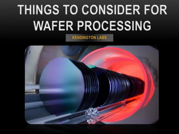
You should learn more about the characteristics and quality of a silicon wafer before buying one. You ought to realize the different cycles engaged with silicon wafer production.

E N D
You should learn more about the characteristics and quality of a silicon wafer before buying one. You ought to realize the different cycles engaged with silicon wafer production. Inspection, coring, polishing, and etching are some of these procedures. These cycles all add to the nature of the result.
Silicon Wafers of High Quality If you’re looking for silicon wafers of high quality, you need to know where to find them. It’s critical to select a silicon wafer of the proper grade because there are numerous varieties. The characteristics of the material will be determined by the manufacturing procedure for silicon wafer coring.
Silicon Wafer Assessment An imperfection map gives data on the deformity size, area, and surface quality. Wafer Inspection requires motion control that is extremely precise and repeatable. Using a specialized inspection tool, it is simple to generate a defect map. The instrument must also be able to measure a semiconductor’s sensitivity. Defect detection tools come in many different varieties, but they all follow the same fundamental principles. We should look into a few of the more well-known varieties. A procedure that is beneficial to semiconductor fabs is substrate mapping. Look for imperfections near a wafer’s edge. It visibly identifies a fault and its location by using color coding. Engineers can use the process to identify critical flaws and enhance the manufacturing procedure. Defect mapping can improve production efficiency at semiconductor fabs. The most important flaws that semiconductors must have are listed below. These tools are used by semiconductor fabs to avoid them.
Silicon Wafer Coring The first step in making a semiconductor is to cut the wafers of silicon into smaller pieces. The production of enormous semiconductor wafers necessitates this, which is also referred to as “die street.” When the silicon has been sliced to the required shape, the wafers are next packaged as either bare die or packaging. Greater precision and control are required for the procedure. The rate at which the substrate is fed into the cutting blade during the cutting process will have an impact on the productivity and yield of the silicon wafer. The possibility of chipping the front of the wafer increases with the rate. Because high-quality chips require high-quality wafers, the procedure is crucial. During the cutting process, the silicon wafer is cut into thin, spherical, and thick pieces. After that, these parts are suitable for making injection-molded tools. A chip made of semiconductors is the result of silicon wafer coring.
Silicon Wafer Cleaning The most vital phase in the cleaning system for silicon wafers is harsh surface cleaning. If you want a surface that is flat and smooth, this step is important. If the surface is not level and smooth, polishing will not be effective. The subsequent stage is to get done with the cleaning. Silicon wafers are minimally roughened during the final polishing step in the wafer dicing service. As a result, the silicon surface’s roughness is decreased to 0.05 nanometers per square centimeter. There are many stages to a polishing step. Silicon wafer producers frequently use the following procedures. The silicon wafer is prepared for the production process by these steps. In the first stage, the silicon wafer is poured into a silicon wave-shaped mold. When silicon ingots are wire-sawed into wafers, kerf, or a gap, can occur. In the second stage, the silicon wafer is polished on both sides, making it simpler for manufacturers to identify which side is used for device production. At last, the silicon wafer is reflected smoothly, with no geography or micro cracks.
Silicon Wafer Reclaiming Silicon wafer reclamation is the process of recovering a silicon wafer from manufacture after it has been treated, cleaned, stripped, and polished. The wafer’s reliability varies with the manufacturing method. In the production of semiconductors, for example, reclaimed wafers can be used in many of the same ways as virgin test wafers. The process of reclaiming semiconductor wafers is complicated. Impurities are removed from the wafers during the etching and gettering processes, which also increase semiconductor yields. Wafers that have been reclaimed are purer than virgin wafers. Additionally, the procedure aids a silicon wafer manufacturer in reducing production expenses. Although these procedures are not brand-new, taken together, they are extremely effective at removing impurities and reclaim silicon wafers during wafer dicing service.
Thin Silicon Wafers For the creation of cutting-edge electronic components, a semiconductor producer produces thin silicon wafers. A semiconductor is made through a complicated process that involves hundreds of millions of tiny parts. The microscopic components can be harmed by even a trace amount of dust. The manufacturer of semiconductors works with ultra-pure silicon crystals in a room with a high vacuum to prevent this. The wafer dicing service relies heavily on the silicon wafers thinness. The surface levelness should be more modest than the profundity of the focal point of the optical lithography openness instruments. Additionally, the standard thickness of a silicon wafer is crucial to the effective production of semiconductors. A thin silicon wafer is said to be several microns thicker than a conventional silicon wafer. A thick silicon wafer, on the other hand, is not considered thin.
Wafers Made of Silicon Carbide The market for silicon carbide is populated by numerous players operating at various points along the value chain. The businesses use a variety of growth techniques to raise their market share. Additionally, they focus on new releases, product development, and collaborations to increase their position in the market. One of the benefits of silicon carbide wafers is their broad bandgap, which is the number of electrons needed to generate a particular semiconductor effect. Silicon carbide is a better choice for applications requiring a high breakdown voltage because of this property.
Wafer Laser Marking A maker of silicon wafers is knowledgeable about the procedures needed to make semiconductors. The silicon wafer is marked by the procedure with lasers. Because it does not require the use of chemicals or inks, the technology is a green process. Lasers are profoundly productive and don’t squander energy. Source: https://techoverdue.com/things-to-consider-in-silicon-wafer-manufacturers/