Download
1 / 8
80 likes | 84 Views
4 LAN-WDM lanes MUX/DEMUX design<br>4 independent full-duplex channels up<br>To 25Gbps data rate per wavelength<br>Hot-pluggable QSFP28 footprint<br>RoHS compliant and Lead Free<br>Up to 10km link length<br>Power dissipation <4.5W (0~70u00b0C)<br>Commercial operating temperature optional

E N D
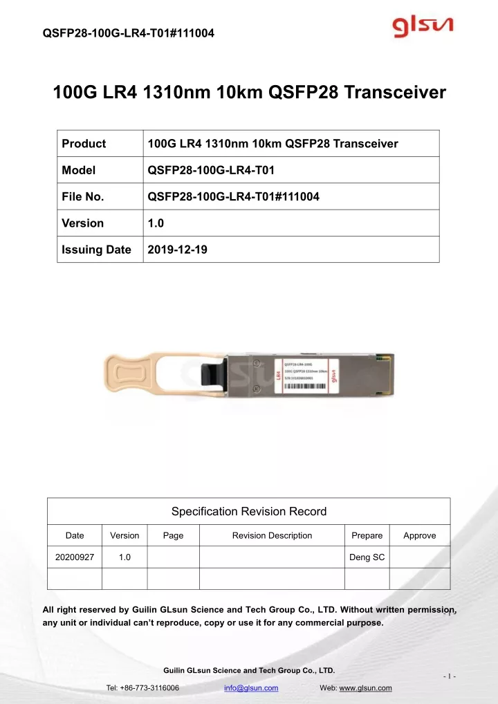
QSFP28-100G-LR4-T01#111004 100G LR4 1310nm 10km QSFP28 Transceiver Product 100G LR4 1310nm 10km QSFP28 Transceiver Model QSFP28-100G-LR4-T01 File No. QSFP28-100G-LR4-T01#111004 Version 1.0 Issuing Date 2019-12-19 Specification Revision Record Date Version Page Revision Description Prepare Approve 20200927 1.0 Deng SC All right reserved by Guilin GLsun Science and Tech Group Co., LTD. Without written permission, any unit or individual can’t reproduce, copy or use it for any commercial purpose. - 1 - Guilin GLsun Science and Tech Group Co., LTD. - 1 - Tel: +86-773-3116006 info@glsun.com Web: www.glsun.com
QSFP28-100G-LR4-T01#111004 Product Feature 4 LAN-WDM lanes MUX/DEMUX design 4 independent full-duplex channels up To 25Gbps data rate per wavelength Hot-pluggable QSFP28 footprint RoHS compliant and Lead Free Up to 10km link length Power dissipation <4.5W (0~70°C) Commercial operating temperature optional Applications 100GBASE-LR4 100GEthernet Regulatory Compliance ESD to the Electrical PINs: compatible with MIL-STD-883 Method 3015 ESD to the Duplex LC Receptacle: compatible with EN 61000-4-2 Immunity compatible with EN 61000-4-3 EMI compatible with FCC Part 15 Class B Laser Eye Safety compatible with FDA 21CFR 1040.10 and 1040.11 IEC 60950, IEC60825-1,2 RoHS compliant with RoHS 2.0(2015/863/EU)-amending Absolute Maximum Rating Parameter Symbol Min Typ Max Unit Maximum Supply Voltage Vcc -0.5 +4.0 V Storage Temperature TS -40 85 °C Operating Humidity RH 0 85 % Recommended Operating Conditions Parameter Symbol Min Typ Max Unit Ref. Power Supply Voltage Vcc 3.13 3.30 3.47 V Power Supply Current Icc 1.36 A Commercial Case Operating Temperature Tc 0 +70 °C Commercial Bit Rate Each Lane BR 25.78 Gbps 9/125um G.652 SMF Lmax 10 km Guilin GLsun Science and Tech Group Co., LTD. - 2 - Tel: +86-773-3116006 info@glsun.com Web: www.glsun.com
QSFP28-100G-LR4-T01#111004 Electrical Characteristics Parameter Symbol Min Typ Max Unit Ref. Transmitter Input differential impedance Rin 90 100 110 Ω 1 Differential data input swing Vin, pp 95 900 mV TX Disable-High Vcc–0.8 Vcc V TX Disable-Low Vee Vee+0.8 V TX Fault-High Vcc-0.8 Vcc V TX Fault-Low Vee Vee+0.8 V Receiver Output differential impedance Rin 90 100 110 Ω 1 Single ended data output swing Vout, pp 900 mV 2 LOS-High Vcc-0.8 Vcc V LOS-Low Vee Vee+0.8 V Notes: 1. AC coupled. 2. Into 100 ohm differential termination. Optical Characteristics Parameter Symbol Min Typ Max Unit Ref. Transmitter Total Average Launch Power PT 10.5 dBm Average Launch Power, each Lane -4.3 +4.5 dBm Optical Modulation Amplitude, each Lane OMA -1.3 +4.5 dBm L0 1294.53 1295.56 1296.59 nm L1 1299.02 1300.05 1301.09 nm Optical Wavelength L2 1303.54 1304.58 1305.63 nm L3 1308.09 1309.14 1310.19 nm Side-Mode Suppression Ratio SMSR 30 dB Extinction Ratio ER 4 dB Guilin GLsun Science and Tech Group Co., LTD. - 3 - Tel: +86-773-3116006 info@glsun.com Web: www.glsun.com
QSFP28-100G-LR4-T01#111004 Receiver RX Sensitivity @25.78Gb/s, each lane SENS -10.6 dBm 1,2 RX Sensitivity(OMA) @25.78 Gb/s, each lane SENS -8.6 dBm 2 Receiver Overload 4.5 nm LOS De-Assert LOSD -12 dBm LOS Assert LOSA -25 dBm LOS Hysteresis 0.5 dB Notes: 1.This value is informative and not the principal indicator of signal strength. A received power below this value cannot be compliant; however, a value above this does not ensure compliance. 2.Measured with PRBS 231-1 at 1E-12BER. Pin Descriptions Pin Symbol Name Ref. 1 GND GND 2 Tx2n Transmitter Inverted Data Input, CML-I 3 Tx2p Transmitter Non-Inverted Data output, CML-I 4 GND GND 5 Tx4n Transmitter Inverted Data Input, CML-I 6 Tx4p Transmitter Non-Inverted Data output, CML-I 7 GND GND The ModSelL is an input pin. When held low by the host, the module responds to 2-wire serial communication commands. The ModSelL allows the use of multiple QSFP+ modules on asingle 2-wire interface bus. When the ModSelL is “High”, the module shall not respond to or acknowledge any 2-wire interface communication from the host. ModSelL signal input node must be biased to the “High” state in the module The ResetL pin must be pulled to Vcc in the QSFP+ module. A low level on the ResetL pin for longer than the minimum pulse length (t_Reset_init) initiates a complete module reset, returning all user module settings to their default state. Module Reset Assert Time (t_init) starts on the rising edge after the low level on the ResetL pin is released. 8 ModSelL 9 ResetL 10 VccRx ﹢3.3V Power Supply Receiver 11 SCL 2-Wire Serial Interface Clock 12 SDA 2-Wire Serial Interface Data Guilin GLsun Science and Tech Group Co., LTD. - 4 - Tel: +86-773-3116006 info@glsun.com Web: www.glsun.com
QSFP28-100G-LR4-T01#111004 13 GND GND 14 Rx3p Receiver Non-Inverted Data Output, CML-O 15 Rx3n Receiver Inverted Data Output, CML-O 16 GND GND 17 Rx1p Receiver Non-Inverted Data Output, CML-O 18 Rx1n Receiver Inverted Data Output, CML-O 19 GND Ground 20 GND Ground 21 Rx2n Receiver Inverted Data Output, CML-O 22 Rx2p Receiver Non-Inverted Data Output, CML-O 23 GND Ground 24 Rx4n Receiver Inverted Data Output, CML-O 25 Rx4p Receiver Non-Inverted Data Output, CML-O 26 GND Ground 27 ModPrsL Module Present, connect to GND The IntL pin is an open collector output and must be pulled to host supply voltage on the host board. The INTL pin is de-asserted “High” after completion of reset, when byte 2 bit 0 (Data Not Ready) is read with a value of ‘0’ and the flag field is read. 28 IntL 29 VccTx +3.3 V Power Supply transmitter 30 Vcc1 +3.3 V Power Supply The LPMode pin shall be pulled up to Vcc in the QSFP+ module. This function is affected by the LPMode pin and the combination of the Power_over-ride and Power_set softwarecontrol bits (Address A0h, byte 93 bits 0,1). 31 LPMode 32 GND Ground 33 Tx3p Transmitter Non-Inverted Data Input, CML-I 34 Tx3n Transmitter Inverted Data Output, CML-I 35 GND Ground 36 Tx1p Transmitter Non-Inverted Data Input, CML-I 37 Tx1n Transmitter Inverted Data Output, CML-I 38 GND Ground Guilin GLsun Science and Tech Group Co., LTD. - 5 - Tel: +86-773-3116006 info@glsun.com Web: www.glsun.com
QSFP28-100G-LR4-T01#111004 Pin-out of Connector Block on Host Board Recommend Circuit Schematic Guilin GLsun Science and Tech Group Co., LTD. - 6 - Tel: +86-773-3116006 info@glsun.com Web: www.glsun.com
QSFP28-100G-LR4-T01#111004 Mechanical Specifications Small Form Factor Pluggable (SFP+) transceivers are compatible with the dimensions defined by the SFP Multi-Sourcing Agreement (MSA) , dimensions are in mm. EEPROM EEPROM memory map specific data field description is as below: Guilin GLsun Science and Tech Group Co., LTD. - 7 - Tel: +86-773-3116006 info@glsun.com Web: www.glsun.com
QSFP28-100G-LR4-T01#111004 Digital Diagnostic Monitoring Interface Five transceiver parameter values are monitored. The following table defines the monitored parameter’s accuracy. Parameter Range Accuracy Calibration Temperature 0 to +70°C (C) ±3°C Internal Voltage 2.97 to 3.63V ±3% Internal Bias Current 0 to 100mA ±10% Internal RX Power -11 to 4.5dBm ±3dB Internal Ordering information Part Number Operating Case temperature DDMI 100G LR4 1310nm 10km QSFP28, Commercial (0~70°C) QSFP28-100G-LR4-T01 Yes Guilin GLsun Science and Tech Group Co., LTD. - 8 - Tel: +86-773-3116006 info@glsun.com Web: www.glsun.com