Download
1 / 11
110 likes | 118 Views
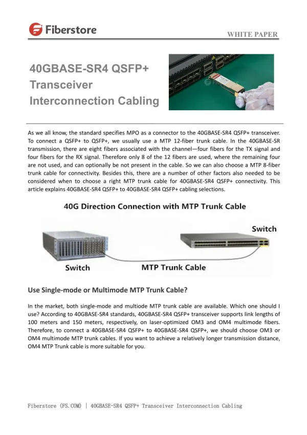
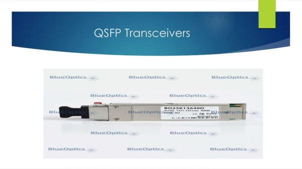
GLSUNu2019s QSFP-40G-ER4-T02 is a transceiver module designed for 40km optical communication<br>applications. The design is compliant to 40GBASE-ER4 of the IEEE P802.3ba standard. The module<br>converts 4 inputs channels (ch) of 10Gb/s electrical data to 4 CWDM optical signals, and multiplexes them<br>into a single channel for 40Gb/s optical transmission. Reversely, on the receiver side, the module optically<br>de-multiplexes a 40Gb/s input into 4 CWDM channels signals, and converts them to 4 channel output<br>electrical data

E N D
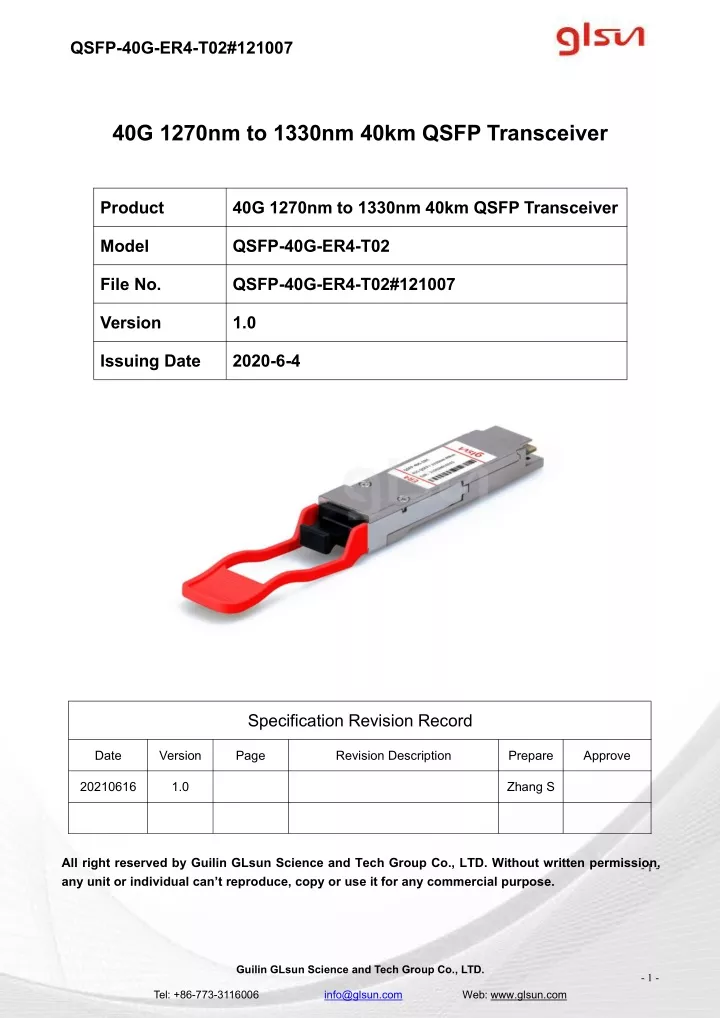
QSFP-40G-ER4-T02#121007 40G 1270nm to 1330nm 40km QSFP Transceiver Product 40G 1270nm to 1330nm 40km QSFP Transceiver Model QSFP-40G-ER4-T02 File No. QSFP-40G-ER4-T02#121007 Version 1.0 Issuing Date 2020-6-4 Specification Revision Record Date Version Page Revision Description Prepare Approve 20210616 1.0 Zhang S All right reserved by Guilin GLsun Science and Tech Group Co., LTD. Without written permission, any unit or individual can’t reproduce, copy or use it for any commercial purpose. - 1 - Guilin GLsun Science and Tech Group Co., LTD. - 1 - Tel: +86-773-3116006 info@glsun.com Web: www.glsun.com
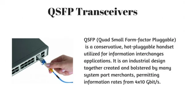
QSFP-40G-ER4-T02#121007 Product Description GLSUN’s QSFP-40G-ER4-T02 is a transceiver module designed for 40km optical communication applications. The design is compliant to 40GBASE-ER4 of the IEEE P802.3ba standard. The module converts 4 inputs channels (ch) of 10Gb/s electrical data to 4 CWDM optical signals, and multiplexes them into a single channel for 40Gb/s optical transmission. Reversely, on the receiver side, the module optically de-multiplexes a 40Gb/s input into 4 CWDM channels signals, and converts them to 4 channel output electrical data. The central wavelengths of the 4 CWDM channels are 1271, 1291, 1311 and 1331 nm as members of the CWDM wavelength grid defined in ITU-T G694.2. It contains a duplex LC connector for the optical interface and a 148-pin connector for the electrical interface. To minimize the optical dispersion in the long-haul system, single-mode fiber (SMF) has to be applied in this module. The product is designed with form factor, optical/electrical connection and digital diagnostic interface according to the QSFP+ Multi-Source Agreement (MSA). It has been designed to meet the harshest external operating conditions including temperature, humidity and EMI interference. Product Feature Duplex LC receptacle optical interface Single +3.3V power supply 4 CWDM lanes MUX/DEMUX design Up to 11.2Gb/s data rate per wavelength Up to 40km transmission on single mode fiber (SMF) Low power dissipation (Max: 3.5W) Built in digital diagnostic function Operating case temperature range: 0℃ to 70℃ Application 40GBASE-ER4 Ethernet Links Infiniband QDR and DDR interconnects Client-side 40G Telecom connections Regulatory Compliance Compliant with 40G Ethernet IEEE802.3ba and 40GBASE-ER4 Standard Compliant with QSFP+ MSA hardware specifications Compliant with RoHS Guilin GLsun Science and Tech Group Co., LTD. - 2 - Tel: +86-773-3116006 info@glsun.com Web: www.glsun.com
QSFP-40G-ER4-T02#121007 Absolute Maximum Ratings Parameter Symbol Min Typ Max Unit Note Supply Voltage Vcc -0.5 +3.6 V Storage Temperature Tst -40 +85 °C Relative Humidity Rh +5 +95 % Recommended Operating Conditions Parameter Symbol Min Typ Max Unit Note Power Supply Voltage Vcc 3.14 3.30 3.46 V Data Rate, each lane 10.3125 11.2 Gb/s Operating Case Temperature Tc 0 - +70 °C Specifications (tested under recommended operating conditions, unless otherwise noted) Parameter Symbol Min. Typ Max. Unit Note Voltage Supply Electrical Characteristics Supply Current Tx Section Icc 1.1 A 1 Rx Section Total Dissipation Power Pw 3.5 W Module power supply noise tolerance 10 Hz -10 MHz (peak-to-peak) Module inrush - initialization time PSNR_Mo d 66 mv T_init 2000 ms Different Signal Electrical Characteristics Single Ended Data Input Swing 190 700 mV Single Ended Data Output Swing 300 850 mV Differential Signal Output Resistance Differential Signal Input Resistance 90 110 Ω 90 110 Ω 3.3V LVTTL Electrical Characteristics Input High Voltage 3.3VIH 2.0 V Guilin GLsun Science and Tech Group Co., LTD. - 3 - Tel: +86-773-3116006 info@glsun.com Web: www.glsun.com
QSFP-40G-ER4-T02#121007 Input Low Voltage 3.3VIL -0.3 V Input Leakage Current 3.3IIN -10 +10 uA Output (IOH=100uA) Output Low Voltage (IOL=100uA) High Voltage 3.3VOH Vcc-0.2 V 3.3VOL 0.2 V Minimum Pulse Width of Control Pin Signal t_CNTL 100 us Transmitter Signaling rate, each lane Gb/s 10.3125 Four Lane Wavelength Range λ1 1264.5 1271 1277.5 nm λ2 nm 1284.5 1291 1297.5 λ3 nm 1304.5 1311 1317.5 λ4 nm 1324.5 1331 1337.5 Total launch power 10.5 dBm Average launch power, each lane Pavg -3.7 +4.5 dBm 2 Optical modulation amplitude, each lane (OMA)2 Difference in launch power between any two lanes (OMA) Extinction ratio OMA -0.7 5 dBm 4.7 dB ER 5.5 dB Side-mode suppression ratio SMSR 30 dB Transmitter and dispersion penalty, each lane Optical return loss tolerance TDP 2.2 dB 20 dB Transmitter reflectance3 –12 dB Transmitter eye mask {X1, X2, X3, Y1, Y2, Y3} {0.25,0.4,0.45,0.25,0.28,0.4} Receiver Receive Rate for Each Lane Gb/s 10.3125 Damage Threshold, each Lane THd 3.8 3 Average Receive Power for Each Lane Receive Power In OMA for Each Lane Difference in Receive Power in OMA between Any Two Lanes Receiver Sensitivity in OMA for Pin -20.2 -1.5 dBm 4, 5 PinOMA -1 dBm 5.5 dBm SOMA -18 dBm 6 Guilin GLsun Science and Tech Group Co., LTD. - 4 - Tel: +86-773-3116006 info@glsun.com Web: www.glsun.com
QSFP-40G-ER4-T02#121007 Each Lane Stressed Receiver Sensitivity in OMA for Each Lane LOS Assert -15.8 dBm 7, 8 -35 dBm LOS Deassert -20 dBm Note: 1. The supply current includes QSFP+ module’s supply current and test board working current. 2. . Average launch power, each lane (min) is informative for 40GBase-ER4, not the principal indicator of signal strength. 3. The receiver shall be able to tolerate , without damage, continuous exposure to an optical input signal having this average power level 4. The average receive power , each lane (max) for 40GBASE-ER4 is larger than the 40GBASE-LR4 transmitter value to allow compatibility with 40GBASE-LR4 units at short distances 5. Average receive power, each lane (min) is informative and not the principal indicator of signal strength. A received power below this value cannot be compliant; however, a value above this does not ensure compliance 6. Receiver sensitivity (OMA), each lane (max) is informative 7. Measured with conformance test signal at TP3 for BER=10-12 8. conditions of stressed receiver sensitivity test: vertical eye closure penalty for each lane is 1.8dB; stressed eye J2 jitter for each lane is 0.3UI; stressed eye J9 jitter for each lane is 0.47UI. Guilin GLsun Science and Tech Group Co., LTD. - 5 - Tel: +86-773-3116006 info@glsun.com Web: www.glsun.com
QSFP-40G-ER4-T02#121007 Pin Description There are 38 contacts intended for high speed signals, low speed signals, power and ground connections. The pin map is shown in Table below. Table: Pin Description Pin Logic Symbol Name/Description Notes 1 VEET [1] Transmitter Ground 2 CML-I Tx2n Transmitter Inverted Data Input 10 3 CML-I Tx2p Transmitter Non-Inverted Data output 10 4 GND Ground 1 5 CML-I Tx4n Transmitter Inverted Data Input 10 6 CML-I Tx4p Transmitter Non-Inverted Data output 10 7 GND Ground 1 8 LVTLL-I ModSelL Module Select 3 9 LVTLL-I ResetL Module Reset 4 10 VccRx +3.3V Power Supply Receiver 2 11 LVCMOS-I/O SCL 2-Wire Serial Interface Clock 5 12 LVCMOS-I/O SDA 2-Wire Serial Interface Data 5 13 GND Ground 1 14 CML-O Rx3p Receiver Non-Inverted Data Output 9 15 CML-O Rx3n Receiver Inverted Data Output 9 16 GND Ground 1 Guilin GLsun Science and Tech Group Co., LTD. - 6 - Tel: +86-773-3116006 info@glsun.com Web: www.glsun.com
QSFP-40G-ER4-T02#121007 17 CML-O Rx1p Receiver Non-Inverted Data Output 9 18 CML-O Rx1n Receiver Inverted Data Output 9 19 GND Ground 1 20 GND Ground 1 21 CML-O Rx2n Receiver Inverted Data Output 9 22 CML-O Rx2p Receiver Non-Inverted Data Output 9 23 GND Ground 1 24 CML-O Rx4n Receiver Inverted Data Output 9 25 CML-O Rx4p Receiver Non-Inverted Data Output 9 26 GND Ground 1 27 LVTTL-O ModPrsL Module Present 6 28 LVTTL-O IntL Interrupt 7 29 VccTx +3.3 V Power Supply transmitter 2 30 Vcc1 +3.3 V Power Supply 2 31 LVTTL-I LPMode Low Power Mode 8 32 GND Ground 1 33 CML-I Tx3p Transmitter Non-Inverted Data Input 10 34 CML-I Tx3n Transmitter Inverted Data Output 10 35 GND Ground 1 36 CML-I Tx1p Transmitter Non-Inverted Data Input 10 37 CML-I Tx1n Transmitter Inverted Data Output 10 38 GND Ground 1 Note: 1. GND is the symbol for signal and supply (power) common for the module. All are common within the module and all module voltages are referenced to this potential unless otherwise noted. Connect these directly to the host board signal-common ground plane. 2. Vcc Rx, Vcc1 and Vcc Tx shall be applied concurrently. Vcc Rx Vcc1 and Vcc Tx may be internally connected within the module in any combination. The connector pins are each rated for a maximum current of 1000 mA. Recommended host board power supply filtering is shown below. Guilin GLsun Science and Tech Group Co., LTD. - 7 - Tel: +86-773-3116006 info@glsun.com Web: www.glsun.com
QSFP-40G-ER4-T02#121007 3. The ModSelL is an input pin. When held low by the host, the module responds to 2-wire serial communication commands. The ModSelL allows the use of multiple modules on a single 2-wire interface bus. When the ModSelL is "High", the module shall not respond to or acknowledge any 2-wire interface communication from the host. ModSelL signal input node shall be biased to the "High" state in the module. In order to avoid conflicts, the host system shall not attempt 2-wire interface communications within the ModSelL de-assert time after any modules are deselected. Similarly, the host shall wait at least for the period of the ModSelL assert time before communicating with the newly selected module. The assertion and de-asserting periods of different modules may overlap as long as the above timing requirements are met. 4. The ResetL pin shall be pulled to Vcc in the module. A low level on the ResetL pin for longer than the minimum pulse length (t_Reset_init) initiates a complete module reset, returning all user module settings to their default state. Module Reset Assert Time (t_init) starts on the rising edge after the low level on the ResetL pin is released. During the execution of a reset (t_init) the host shall disregard all status bits until the module indicates a completion of the reset interrupt. The module indicates this by asserting "low" an IntL signal with the Data_Not_Ready bit negated. Note that on power up (including hot insertion) the module should post this completion of reset interrupt without requiring a reset. 5. Low speed signaling other than SCL and SDA is based on Low Voltage TTL (LVTTL) operating at Vcc. Vcc refers to the generic supply voltages of VccTx, VccRx, Vcc_host or Vcc1.Hosts shall use a pull-up resistor connected to Vcc_host on each of the 2-wire interface SCL (clock), SDA (data), and all low speed status outputs. The SCL and SDA is a hot plug interface that may support a bus topology. 6. ModPrsL is pulled up to Vcc_Host on the host board and grounded in the module. The ModPrsL is asserted "Low" when inserted and deasserted "High" when the module is physically absent from the host connector. 7. IntL is an output pin. When IntL is "Low", it indicates a possible module operational fault or a status critical to the host system. The host identifies the source of the interrupt using the 2-wire serial interface. The IntL pin is an open collector output and shall be pulled to host supply voltage on the host board. The INTL pin is deasserted "High" after completion of reset, when byte 2 bit 0 (Data Not Ready) is read with a value of '0' and the flag field is read (see SFF-8636). 8. The LPMode pin shall be pulled up to Vcc in the module. The pin is a hardware control used to put modules into a low power mode when high. By using the LPMode pin and a combination of the Power_override, Power_set and High_Power_Class_Enable software control bits (Address A0h, byte 93 bits 0,1,2), the host controls how much power a module can dissipate. Guilin GLsun Science and Tech Group Co., LTD. - 8 - Tel: +86-773-3116006 info@glsun.com Web: www.glsun.com
QSFP-40G-ER4-T02#121007 9. Rx(n)(p/n) are module receiver data outputs. Rx(n)(p/n) are AC-coupled 100 Ohm differential lines that should be terminated with 100 Ohm differentially at the Host ASIC(SerDes). The AC coupling is inside the module and not required on the Host board. For operation at 28 Gb/s the relevant standards (e.g., OIF CEI v3.1) define the signal requirements on the high-speed differential lines. For operation at lower rates, refer to the relevant standards. 10. Due to the possibility of insertion of legacy QSFP and QSFP+ modules into a host designed for higher speed operation, it is recommended that the damage threshold of the host input be at least 1600 mV peak to peak differential. Output squelch for loss of optical input signal, hereafter Rx Squelch, is required and shall function as follows. In the event of the optical signal on any channel becoming equal to or less than the level required to assert LOS, then the receiver data output for that channel shall be squelched or disabled. In the squelched or disabled state output impedance levels are maintained while the differential voltage swing shall be less than 50 mVpp. In normal operation the default case has Rx Squelch active. Rx Squelch can be deactivated using Rx Squelch Disable through the 2-wire serial interface. Rx Squelch Disable is an optional function. For specific details refer to SFF-8636. 11. Tx(n)(p/n) are module transmitter data inputs. They are AC-coupled 100 Ohm differential lines with 100 Ohm differential terminations inside the module. The AC coupling is inside the module and not required on the Host board. For operation at 28 Gb/s the relevant standards (e.g., OIF CEI v3.1) define the signal requirements on the high-speed differential lines. For operation at lower rates, refer to the relevant standards. Due to the possibility of insertion of modules into a host designed for lower speed operation, the damage threshold of the module input shall be at least 1600 mV peak to peak differential. Output squelch, hereafter Tx Squelch, for loss of input signal, hereafter Tx LOS, is an optional function. Where implemented it shall function as follows. In the event of the differential, peak-to-peak electrical signal on any channel becomes less than 50 mVpp, then the transmitter optical output for that channel shall be squelched or disabled and the associated TxLOS flag set. Where squelched, the transmitter OMA shall be less than or equal to -26 dBm and when disabled the transmitter power shall be less than or equal to -30 dBm. For applications, e.g. Ethernet, where the transmitter off condition is defined in terms of average power, disabling the transmitter is recommended and for applications, e.g. InfiniBand, where the transmitter off condition is defined in terms of OMA, squelching the transmitter is recommended. In module operation, where Tx Squelch is implemented, the default case has Tx Squelch active. Tx Squelch can be deactivated using Tx Squelch Disable through the 2-wire serial interface. Tx Squelch Disable is an optional function. For specific details refer to SFF- 8636. Guilin GLsun Science and Tech Group Co., LTD. - 9 - Tel: +86-773-3116006 info@glsun.com Web: www.glsun.com
QSFP-40G-ER4-T02#121007 Recommended Host Board Schematic Guilin GLsun Science and Tech Group Co., LTD. - 10 - Tel: +86-773-3116006 info@glsun.com Web: www.glsun.com
QSFP-40G-ER4-T02#121007 Recommended Power Supply Filter Ordering Information Part Number Description QSFP-40G-ER4-T02 QSFP+ ER4, 40G 1270nm~1330nm 40km DDM, 0℃ to 70℃ Guilin GLsun Science and Tech Group Co., LTD. - 11 - Tel: +86-773-3116006 info@glsun.com Web: www.glsun.com