Download
1 / 1
0 likes | 22 Views
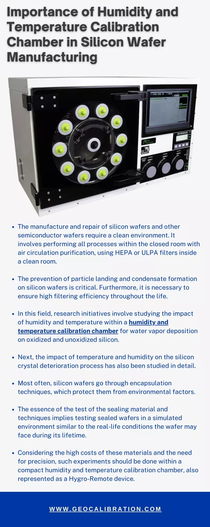
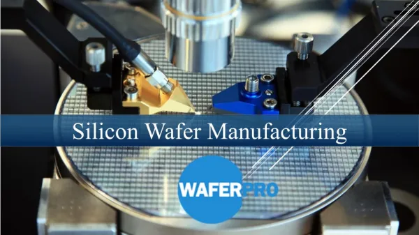
In this field, research initiatives involve studying the impact of humidity and temperature within a humidity and temperature calibration chamber for water vapor deposition on oxidized and unoxidized silicon.<br>

E N D
The manufacture and repair of silicon wafers and other semiconductor wafers require a clean environment. It involves performing all processes within the closed room with air circulation purification, using HEPA or ULPA filters inside a clean room. The prevention of particle landing and condensate formation on silicon wafers is critical. Furthermore, it is necessary to ensure high filtering efficiency throughout the life. In this field, research initiatives involve studying the impact of humidity and temperature within a humidity and temperature calibration chamber for water vapor deposition on oxidized and unoxidized silicon. Next, the impact of temperature and humidity on the silicon crystal deterioration process has also been studied in detail. Most often, silicon wafers go through encapsulation techniques, which protect them from environmental factors. The essence of the test of the sealing material and techniques implies testing sealed wafers in a simulated environment similar to the real-life conditions the wafer may face during its lifetime. Considering the high costs of these materials and the need for precision, such experiments should be done within a compact humidity and temperature calibration chamber,also represented as a Hygro-Remote device. WWW.GEOCALIBRATION.COM


![The Importance of Humidity Calibration in Data Logging[08-feb]](https://cdn7.slideserve.com/12904177/in-the-world-of-data-logging-precision-dt.jpg)