GAN EPITAXIAL WAFERS MARKET ANALYSIS: Exploring Future Growth by 2027
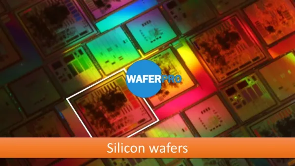
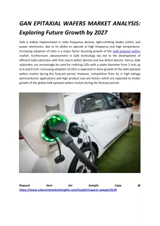
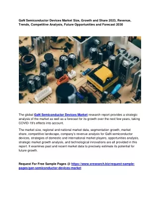
GaN is widely implemented in radio frequency devices, light-emitting diodes (LEDs), and power electronics, due to its ability to operate at high frequency and high temperature. Increasing adoption of LEDs is a major factor boosting growth of the GaN epitaxial wafers market. Furthermore, advancement in GaN technology has led to the development of efficient GaN substrates with free macro defect density and low defect density. Hence, GaN substrates can increasingly be used for realizing LEDs with a wafer diameter from 2 inch up to 6 and 8 inch. Increasing adoption of LEDs is expected to drive growth of the GaN epitaxial wafers market during the forecast period. However, competition from Sic in high-voltage semiconductor applications and high product cost are factors which are expected to hinder growth of the global GaN epitaxial wafers market during the forecast period. Request here for Sample Copy @ https://www.coherentmarketinsights.com/insight/request-sample/3219 Global GaN Epitaxial Wafers Market Competitive Background: Key players in the global GaN epitaxial wafers market are RF Globalnet, Aixtron, EpiGaN nv, Sciocs, Semiconductor Wafer Inc. IGSS GaN, SweGaN, NTT Advanced Technology Corporation, Infineon Technologies AG, Mitsubishi Electric Corporation, Toshiba Infrastructure Systems & Solutions Corporation, Koninklijke Philips N.V., and ALLOS Semiconductors GmbH among others. Global GaN Epitaxial Wafers Market Taxonomy: On the basis of wafer size, the global GaN epitaxial wafers market is segmented into: u2022t2-Inch Wafer u2022t4-Inch Wafer u2022t8-Inch and Above Wafer On the basis of application, the global GaN epitaxial wafers market is segmented into: u2022tLEDs u2022tLasers u2022tRadio Frequency Devices u2022tPower Drives u2022tTransistors u2022tOthers On the basis of region, the global GaN epitaxial wafers market is segmented into: u2022tNorth America u2022tEurope u2022tAsia Pacific u2022tLatin America u2022tMiddle East u2022tAfrica Download PDF Brochure Here @ https://www.coherentmarketinsights.com/insight/request-pdf/3219 Regional Insight: In terms of geography, Asia Pacific is expected to be dominant in the global GaN epitaxial wafers market during the forecast period. This is owing to wide utilization of GaN-based transistors in the defense and military sector, increasing demand for LEDs from various industries such as consumer electronics & automotive and increasing renewable energy generation in the region. For instance, in June 2019, Samsung announced the launch of The Wall Luxury GaN micro-LED display configurable from 73u201d in 2K to 292u201d in 8K. Moreover, Asia Pacific region is expected to witness significant growth over the forecast period, which can be attributed to high adoption of innovative technologies such as epi-nucleation, buffer structure technology etc. An epitaxial wafer also known as, epi wafer, is a wafer of semiconducting material made by epitaxial growth (epitaxy) for use in photonics, microelectronics, spintronics, or photovoltaic. The epitaxial layers consist of various compounds such as gallium nitride (GaN), gallium arsenide (GaAs), or some combination of the elements gallium, indium, aluminum, nitrogen, phosphorus or arsenic. High electron mobility, low switching losses, and fewer lattice mismatches are some of the key advantages of GaN Substrate, which are leading its adoption in industries such as power electronics and optoelectronics. About Coherent Market Insights: Coherent Market Insights is a prominent market research and consulting firm offering action-ready syndicated research reports, custom market analysis, consulting services, and competitive analysis through various recommendations related to emerging market trends, technologies, and potential absolute dollar opportunity.t Contact Us: Name: Mr. Raj Shah Phone: US 12067016702 / UK 4402081334027 Email: sales@coherentmarketinsights.com Visit Our Blogs: https://blog.coherentmarketinsights.com
42 views • 3 slides