Download

1 / 13
130 likes | 688 Views
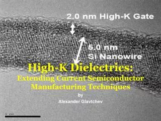
High-K Dielectrics The Future of Silicon Transistors. Matthew Yang EECS 277A Professor Nelson. Outline. Introduction Problem with SiO 2 Solution: High-K Dielectric High-K Dielectric Performance Manufacturing Process Summary. Introduction. Continual size reduction of transistors.

E N D
High-K DielectricsThe Future of Silicon Transistors Matthew Yang EECS 277A Professor Nelson
Outline • Introduction • Problem with SiO2 • Solution: High-K Dielectric • High-K Dielectric Performance • Manufacturing Process • Summary
Introduction • Continual size reduction of transistors. • Decrease in channel length. • Decrease in gate dielectric thickness.
Introduction • Currently, gate dielectric approaching thickness of a few atoms. • Problem: Quantum Mechanics • Electron tunneling gate current leakage • With the number of transistors on a single chip growing exponentially, power dissipation becomes a big problem.
Problem with SiO2 • SiO2 layer is too thin. • 90nm node has a dielectric thickness of 1.2nm. • Low relative dielectric constant. • If there is to be any increase in performance, an alternative must be found. Image courtesy of Intel.
Solution: High-K Dielectric • Options: • Increase dielectric thickness. • Increase relative dielectric constant. • High-k dielectrics are a logical solution.
Solution: High-K Dielectric • Problems with high-k/poly-si: • Increased threshold voltage Image courtesy of Intel.
Solution: High-K Dielectric • Problems with high-k/poly-si: • Increased threshold voltage • Decreased channel mobility Image courtesy of Intel.
Solution: High-K Dielectric • Replace poly-si gates with doped, metal gates. • Improved mobility. Image courtesy of Intel. Image courtesy of Intel.
High-K Dielectric Performance • Performance with high-k dielectric and metal gate: Image courtesy of Intel.
Manufacturing Process • Several types of high-k dielectric: HfO2, ZrO2, TiO2. • Chemical vapor deposition: Image courtesy of Intel.
Summary • As transistors shrink in size, an alternative to SiO2 must be found. • HfO2, in conjunction with metal gates, improves leakage current, gate capacitance, and speed. • By replacing SiO2 with HfO2, transistors will be able to continue to shrink without sacrificing performance.
Sources Chau, Robert, et. al. "Application of High-K Dielectrics and Metal Gate Electrodes to Enable Silicon and Non-Silicon Logic Nanotechnology." Microelectronic Engineering. Vol.80 (2005): 1-6. Chau, Robert. "Role of High-k Gate Dielectrics and Metal Gate Electrodes in Emerging Nanoelectronic Devices." 14th Biennial Conference on Insulating Films on Semiconductors 2005. Leuven, Belgium. 22-24 June 2005. Chau, Robert. "Gate Dielectric Scaling for High-Performance CMOS: from SiO2/PolySi to High-k/Metal-Gate." International Workshop on Gate Insulator 2003. Tokyo, Japan. 6-7 November 2003. Chau, Robert, et. al. "High-k/Metal-Gate Stack and Its MOSFET Characteristics" _IEEE Electron Device Letters_. 25:6 (June 2004): 408-410. Intel (4 November 2003). "Intel's High-K/Metal Gate Announcement." Press Release. Retrieved on 2008-11-03.