Download

1 / 11
110 likes | 122 Views
This block diagram illustrates the control flow and signals involved in testing the Read Master component, Register File, and CPU interaction. The process involves issuing read requests on the bus, checking for readiness, and managing data flow to and from the Dual Port Memory. Critical signals such as Clk, Resetn, Address, Read, and Readdata are shown in the diagram. By enabling the master interface, reading data from on-chip memory, and writing output to the Dual Port Memory, the CPU can verify results effectively. Implementation notes highlight Byte addressing in the NIOS2 system and address considerations when reading data from the bus.

E N D
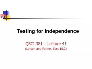
Block diagram Register File 1 CPU 2 Read_master 1 3 Dual Port Memory 4
Finite State Machine Issue Read request on bus ADDR>length / Done !waitrequest waitrequest !ADDR>length Write DP Done
Control Flow diaGram Start Address > Length? Output Done signal yes no Send Address Read from bus no Data Ready? yes Write to DPRAM
Avalon Master read signal • Once we assert the address and read signals, if the waitrequest is low, we can read data from the bus.
Control flow • CPU enable the master interface via MMIO to the register file • Master read data from on-chip memory through AVALON bus • Master write the output to the Dual port memory. Repeat 2 and 3 until length • CPU verify the result on DP memory.
Master Signals • Clk : GS , 1 • Resetn : GS , 1 • Waitrequest : MS , 1 • Address : MS , 32 • Read : MS , 1 • Readdata : MS , 32
Avalon_min signals Clk Resetn enable Readdata waitrequest Addr_bass Addr_length Address Read DP_address DP_wdata DP_write DP_enable done Avalon read master interface
Memory map IO address • 3’b000 : addr_bass • 3’b001 : addr_length • 3’b010 : enable • 3’b011 : done
Implementation note • NIOS2 system is Byte address. If we want to read a word(4 bytes) on the bus, we have to take about the address ourselves.