Download
1 / 18
180 likes | 346 Views
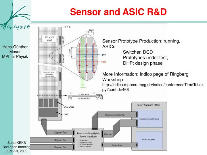
Sensor and ASIC R&D. Sensor Prototype Production: running, ASICs: Switcher, DCD Prototypes under test, DHP: design phase More Information: Indico page of Ringberg Workshop: http://indico.mppmu.mpg.de/indico/conferenceTimeTable.py?confId=466. Sensor Production Status.

E N D
Sensor and ASIC R&D Sensor Prototype Production: running, ASICs: Switcher, DCD Prototypes under test, DHP: design phase More Information: Indico page of Ringberg Workshop: http://indico.mppmu.mpg.de/indico/conferenceTimeTable.py?confId=466
Sensor Production Status Status at 2nd Belle II meeting (March): SOI wafer bonding at Tracit, France 30 SOI wafers received, processing in our own lab has started Presently: cleaning, oxygenation, alignment mask, first implantation: next week. Processed are 6 wafers + dummies
Wafer layout Small test matrices with various pixel sizes; 50 µm x 50 µm .. 50 µm x 175 µm Technology variations (gate length L) 4 ½ module large matrices with most likely pixel sizes 5cm: 50µm x 75µm 5cm: 50µm x 100µm 3.5cm 50µm x 50µm 3.5cm 50µm x 75µm Important for timing!
Pixel Drain Gate Clear Source Favorized design (zoom)
Option: common source/drain: very compact (small pitch) but interleaved readout 1 1 2 2 3 3 5 5 6 6 7 7 8 8 4 4 3 2 3 3 2 2 3 2 5 4 4 5 4 5 5 4 7 7 7 7 6 6 6 6 8 8 1 8 1 8 1 1 To gate switcher To DCD Source (all connected, double pixel share one source) Drain (neighbour pixel share one drain, connected to one DCD channel) Gate (double pixel have gates connected & interleaved connection)
1. row 2. row 3. row clear clear clear gate gate gate drain current “1“ “0“ “0“ “1“ “0“ “0“ DEPFET parameter model Read-Clear-Read for 3 neighboring matrix rows Including realistic RC loads for control and readout lines RC times critical: 80 ns sample-clear-sample just ok Capacitance depends on sensor length (drain lines) and number of pixels (drain capacitance)
Changes for final production Thin oxides: for improved radiation hardness: dox 200nm -> 100nm => small threshold voltage shifts => however: reduction of gain Shorter gates compensate gain loss due to thin oxide -> compensate by reducing L by 0.8 (6 µm -> 4.7 µm) improve gain (overcompensate) L ~ 4.0µm: gq ~ 600 pA/e (instead of 450 pA/e) needs plasma etching Tests/test structures on PXD6 production Extra thin oxide test planned in autumn
DEPFET Readout and Control ASICs DCD, Switcher: Heidelberg DHP: Bonn, Barcelona
9V ‘SRAM’ 6V ‘SRAM’ 3V out 6V ‘SRAM’ 3V ‘SRAM’ 0V Switcher 3 Switcher 3 Radiation tolerant layout in 0.35 μm technology 128 channels + Very fast - Operation up to 11.5 V Novel design: Uses stacked LV transistors, HV twin-wells and capacitors as level-shifters + No DC power consumption Tested up to 22 Mrad 2ns 9V
Switcher 4 Switcher 4 Uses radiation tolerant high voltage transistors in HV 0.35 μm technology 64 channels + fast enough + Possible operation up to 50 V (30V tested) + low DC power consumption Enclosed design of NMOS HV transistors Should be rad hard (to be tested) Final chip: only 16 or 32 channels
DCD • - Technology 0.18 μm • - 72 Channels • - 2 ADCs and regulated cascode/channel • - 6 channels multiplexed to one digital LVDS output • - ADC sampling period 160 ns (8 bits) • - Channel sampling period 80 ns • - LVDS output: 600 M bits/s • - Chip: 7.2 G bits/s (12 outputs) • - Radiation tolerant design • - ~ 1mW/ADC
DCD Radiation hardness tested up to 7 Mrad Layout for Belle II: 160 channel chip, bump bonded
DCD Tests Manuel Koch, Bonn • Works almost at design frequency (540 MHz: 88ns line rate) • (works still at nominal 600 MHz, but with higher noise) • Noise level: 90nA with 450 pA/e: 200 e ENC (S/N = 20:1) • Some bugs discovered, improved version will be submitted • Push DEPFET gain (600 pA/e ?)
DHP Configuration Synchronization DCD/Switcher Data processing (CM, Pedestal 0-Sup) Clustering? Buffering, Trigger handling Being designed, 90nm CMOS
DHP – Signal Rates & Data Flow Assumptions ( extended specs.) • 10µs r/o time ( 20 µs) • 128 switcher channels ( 256) • 10 kHz trigger (un-triggered r/o) • 2-4% occupancy Bonn, Barcelona
Summary: ASICs • - DCD prototype chip has been tested with test signals that correspond to DEPFET currents and irradiated up to 7 Mrad. • The chip works fine and has high enough conversion speed. • Operation with matrices still to be tested – we do not expect problems. • Only „fine tuning“ of the design for the super KEKB operation is necessary. • - Switcher prototype with LV transistors has been tested and irradiated up to 22 MRad. • The chip works fine and has adequate speed for Belle II operation. • - Another prototype with HV transistors has been designed and tested. • - The irradiation of the chip still has to be done but the basic and most critical part (high-voltage NMOS) has been irradiated up to 600 KRad and no damage has been observed. • - DHP chip will be designed using digital design tools in intrinsically radiation hard 90 nm technology. • - Choice between 4 different bumping technologies – advantages and disadvantages still to be evaluated • Planned submissions: • Switcher: October 09 • DCD: September 09 • DHP: October 09
Questions General: Radiation: SEU tolerance: what level of background from hadrons? Ground loops? DHP Trigger: max. rate and trigger dead time Interleaved readout: not wanted by ASIC designers Distance DHP-DHH How many (complete) frames to store (for calibration) Switcher: Range of different operation voltages (compatible with internal level shifter)