Download
1 / 18
180 likes | 312 Views
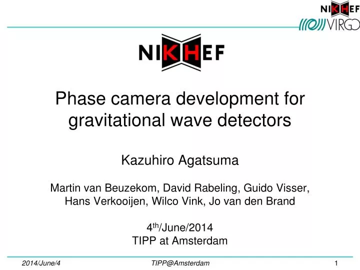
Phase camera development for gravitational wave detectors. Kazuhiro Agatsuma Martin van Beuzekom , David Rabeling , Guido Visser , Hans Verkooijen , Wilco Vink , Jo van den Brand 4 th /June/2014 TIPP at Amsterdam. Contents. Phase camera is prepared for Advanced VIRGO Background

E N D
Phase camera development for gravitational wave detectors Kazuhiro Agatsuma Martin van Beuzekom, David Rabeling, Guido Visser, Hans Verkooijen, WilcoVink, Jo van den Brand 4th/June/2014 TIPP at Amsterdam TIPP@Amsterdam
Contents Phase camera is prepared for Advanced VIRGO • Background • Gravitational waves • GW detector • VIRGO • Marginally stable power recycling cavity • Phase camera • Principle • Setup plan in AdV • Prototype experiment at Nikhef • Selection of components • Summary and plan TIPP@Amsterdam
Gravitational waves • Predicted by A. Einstein (1916) • Nobody detect it directly yet • Indirect evidence • Hulse and Taylor pulsar (1974) • => Nobel prize (1993) • BICEP2 (2014 in discussion) • Direct observations will make a new method to observe universe • Binary neutron star • Black hole • Super nova • Inflation • Unknown source • etc… • General relativity • Beginning of universe Gravitational waves y z x TIPP@Amsterdam
Gravitational wave detector Michelson Interferometer y Fabry-Perot Michelson Interferometer Power recycled Fabry-Perot Michelson Interferometer x Dual recycled Fabry-Perot Michelson Interferometer Power recycling mirror BS Laser EOM Fabry-Perot Cavity fp Signal recycling mirror Input Mode Cleaner Output Mode Cleaner Modulation-Demodulation (Pound–Drever–Hall technique) is used to operate IFO (control position and angle) Photo detector TIPP@Amsterdam
VIRGO Nikhef contributes to VIRGO (Collaboration between France, Italy, Netherlands, Poland and Hungary) Upgrade VIRGO => advanced VIRGO (AdV) (Italy, Pisa) [http://www.ego-gw.it/public/about/welcome.aspx] • Worldwide competition to the first detection • LIGO (USA) • KAGRA (Japan) • After the first detection • World competition => World corroboration TIPP@Amsterdam
Marginally stable recycling cavity • VIRGO uses marginally stable recycling cavity • Degeneration of higher order modes (HOMs) • (Sideband power reduction can easily happen by aberration of mirrors) • Control becomes unstable • Aberrations • Thermal lens • Substrate inhomogeneities • Surface shape errors ITM CO2 laser Wave front sensor ITM PRM BS Pick-off Solution: Thermal Compensation System (TCS) Sensor: Phase camera, Actuator: CO2 laser with compensation plate TIPP@Amsterdam
Phase Camera • Frequency selective wave front sensor • Heterodyne detection • Pin-hole scanning IFO (Pick-off mirror in IFO) PM for IFO EOM Test beam (with PM: fp) fp BS Demodulation fH, fH+fp, fH-fp AOM Reference beam (Frequency shift by fH) fH I Scanner Q Pin-hole Mapping of amplitude and phase TIPP@Amsterdam
Setup plan in AdV Phase camera will be placed on three ports PC1: Input beam [f1 - f5] PC2: Power recycling cavity [f1, f4] PC3: Output beam [f2] PC1 CO2 laser PC2 EOM IMC PC3 : Arm cavity control (common) : SRC : PRC : Support for f1 : Input MC OMC Five sidebands will be used TIPP@Amsterdam
Setup plan in AdV Frequency shifter: Fiber coupled AOM PC1: Input beam (Injection bench) PC2: Power recycling cavity (B4) PC3: Output beam (B1p) TIPP@Amsterdam
Prototype test at Nikhef - Current setup - • Test beam: Phase modulator (EOM): DC -> 250 MHz • Reference beam: Frequency shift (AOM): 80 MHz • Scanner: Galvanometer (GVS012) • Photo-detector : New focus 1811 (125 MHz) • DSP: • LAPP fast ADC/FPGA board (400MHz Clock) • AdV Real-time system signal processing Each sideband is selective TIPP@Amsterdam
Prototype test at Nikhef Laser EOM AOM Galvanometer PD TIPP@Amsterdam
Mapping result (preliminary) Carrier • Test beam: 10MHz PM • Power ratio (test beam and reference beam) is not optimized here => Calculation of SNR using actual parameters is in progress • The phase between carrier and sidebands should be identical in the ideal IFO => Subtraction of those shows aberration map! Test Reference USB TIPP@Amsterdam
Scanning pattern (Archimedes' spiral) 32 x 32 pixels: 16 Hz 128 x 128 pixels: 64 Hz 256 x 256 pixels: 128 Hz In the case of the total acquisition time of 1 second to make one pattern (According to a simulation, a total acquisition time of at least 2-5 s [0.03 s] is necessary in order to keep sufficient precision of the phase measurement) Standard aperture diameter: 5 mm Test beam size: w = (2.5) / 3 = 833 um Quickest acquisition is 0.25 s (128 x 128 pixels, 256 Hz) with our scanner (Requirement: 100 x 100 pixels) TIPP@Amsterdam
Scanner (PZT scanner) ~300 Hz 5mm PD 20 cm • Tilt angle range: • 50 mrad(±25 mrad) • to scan 5 mm range, • a half a maximum voltage is necessary with 20 cm distance • The quickest operation is 300 Hz TIPP@Amsterdam
Photodiode board New PD has been developed atNikhef (close to completion) Flat response up to 700MHz • FCI-InGaAs-55 • Active area diameter = 55 mm (pin-hole) • NEP 2.66e-15 W/rtHz • Flat window, AR coated • DC output and • RF TIA: HITTITE 799LP3E • 10 kOhm • DC – 700MHz • 46 nV/rtHz output noise (spec) • = 4.6 pA/rtHz input referrred • Shot noise limited if Idiode > ~66 uA (VIR-0439A-13) TIPP@Amsterdam
Digital demodulation board 11x ‘DFT-slice’ I • Digital Demodulation at 11 (fixed) frequencies (fh+/f1..f5) in parallel • 14 bit ADC at 500 MS/s + Xilinx Virtex-7 FPGA • Measure phase (and power) using 16k samples per ‘pixel’ • can measure 32 k ‘pixels’ per second, frequency resolution ~30 kHz • Best resolution when using external ref. frequencies (i.e. diff. phase measurement) • s = ~0.3 mRad at 211 MHz ADC PD in atan power fh +/-f1..f5 to DAQ block Q Hann* cosine LUT 16k Hann* sine LUT 16k sample clock cntr 0..N-1 Df I fh ADC atan fh +/-f1..f5 f1..f5 Q (VIR-0439A-13) TIPP@Amsterdam
Optical layout design (PC1) z=0 (※) preliminary design Optical layout is in progress TIPP@Amsterdam
Summary and Plan Summary • Phase camera can observe wave fronts for each PM sideband => Useful monitor for TCS in Virgo • Prototype experiment is on going • Component selection has done • High speed PD and digital board are being prepared at Nikhef Plan (in progress) • SNR calculation using actual parameters • Optical layout drawings TIPP@Amsterdam