Download
1 / 14
160 likes | 637 Views
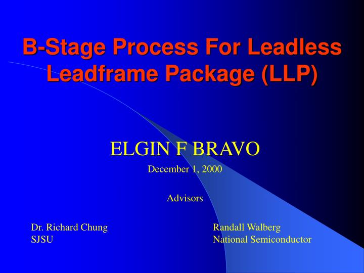
B-Stage Process For Leadless Leadframe Package (LLP). ELGIN F BRAVO December 1, 2000 Advisors Dr. Richard Chung Randall Walberg SJSU National Semiconductor. LLP. MDIP. Leadless Leadframe Package. Project Objective.

E N D
B-Stage Process For Leadless Leadframe Package (LLP) ELGIN F BRAVO December 1, 2000 Advisors Dr. Richard Chung Randall Walberg SJSU National Semiconductor
LLP MDIP Leadless Leadframe Package
Project Objective • To reduce current LLP size from 3.0mm x 3.0mm to 2.0mm x 2.0mm in order to stay completive in the small appliance market.
0.5 mm 0.3 mm Proposed Solution
Epoxy Bleeding 0.3mm
Proposed Solution To Epoxy Bleeding Stencil coat back of wafers with a thin layer of B-stage epoxy.
Properties Of B-stage Epoxy • Stencil or screen printable. • B-stageable or semicures at low temp (~100C), which removes tackiness. • Shelf life of 6 months @ 25C after semicuring. • Becomes tacky again at a 150C. • Completely cures or C-stageable at 180C.
Objectives Of 1st Experiment • Determine if a 0.5mm layer of epoxy can be successfully applied onto wafer. • Determine if backcoated die can be successfully die attach onto leadframe. • Determine epoxy bond strength by conducting die shear test .
Results From B-Stage Process B-Stage process Regular process
Shear (B-Stage epoxy) Shear (Standard epoxy) F F Die Shear
Future Experiments • Wirebonding process • Board level reliability • Electrical testing • Moisture sensitivity level • Thermal cycling
Conclusion • Backcoated die with B-Stage epoxy was successfully die attached. • Die shear test will be done by end of December. • Wirebonding is scheduled to begin in early January. • Board level reliability tests will start in early April.