Download
1 / 12
130 likes | 269 Views
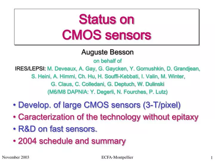
Status on CMOS sensors. Auguste Besson on behalf of IRES/LEPSI: M. Deveaux, A. Gay, G. Gaycken, Y. Gornushkin, D. Grandjean, S. Heini, A. Himmi, Ch. Hu, H. Souffi-Kebbati, I. Valin, M. Winter, G. Claus, C. Colledani, G. Deptuch, W. Dulinski (M6/M8 DAPNIA: Y. Degerli, N. Fourches, P. Lutz).

E N D
Status onCMOS sensors Auguste Besson on behalf of IRES/LEPSI: M. Deveaux, A. Gay, G. Gaycken, Y. Gornushkin, D. Grandjean, S. Heini, A. Himmi, Ch. Hu, H. Souffi-Kebbati, I. Valin, M. Winter, G. Claus, C. Colledani, G. Deptuch, W. Dulinski (M6/M8 DAPNIA: Y. Degerli, N. Fourches, P. Lutz) • Develop. of large CMOS sensors (3-T/pixel) • Caracterization of the technology without epitaxy • R&D on fast sensors. • 2004 schedule and summary ECFA-Montpellier
History • MIMOSA 1,2,4,5 tested at CERN-SPS with 120 GeV/c - • M6 tests in progress • M7 available soon • SUCESSOR 2 (SUCIMA PROJECT): beam test in 2003 • 40 m pitch, no epitaxial layer. • 2003: M4, M5, M6 tests, M7 fabricated A. Besson, ECFA-Montpellier
3-T/pixel large CMOS sensors(M5) • AMS 0.6 m (M1 like) • reticle size 19.4 x 17.4 mm2 • 512 x 512 pixels (/ each of 4 matrices) • 17x17 m pitch • 4 sub-matrices per sensors, read-out in parallel • 6 wafers (6’’) built in 2001 • 3 wafers thinned down to 120m (2 in 2003) • 2002 results: • Yield 20-30 % • det ≳ 99%; sp ~1.7 m; <gain> ~0.2% A. Besson, ECFA-Montpellier
3-T large sensors: 2003(2) • Beam test at SPS (2003) • 3 sensors • 120 GeV/c - • Performance uniformity tests • between sub-matrices, sensors • diode size comparisons Small diode (3x3 m2) Big diode (5x5 m2) A. Besson, ECFA-Montpellier
3-T large sensors: results(3) • submatrices have similar properties • ~1 dead column / 512 (i.e. ~0.2% det inefficiency) • single point resolution ≲ 2.5 m (still improvable) • Effect of particle incidence • chip turned w.r.t. beam direction • charge as expected A. Besson, ECFA-Montpellier
3-T large sensors: M5-B (4) • Mimosa 5-B • 23 wafers produced in oct. 2003 • Slightly improved fabrication process (metalisation) • should reduce dead columns rate. • should improve rate of good chips (yield) • setting up thinning to 15 m (Nov 03) (with a Si wafer on the electronics side for handling) • Application to bio-medical imaging (20-30 keV e-) A. Besson, ECFA-Montpellier
3-T large sensors: application (5) • STAR: extension of the Vertex Detector (2006) • charm physics small radius, granular and thin detector • 2 pixel layers ≳ 1000 cm2R(layer 1) ≳ 2 cm ; R(layer 2) ≲ 4 cm ; • M5 performances are close to the STAR requirements • started a collaboration with LBL (and BNL) • first MIMO⋆1 prototype in summer 2004 (new TSMC 0.25 m tech.) • Requirements • pt~ 3 m • 2.6 kRad/year • 2.1010 neq/cm2/year • read out time 10-20 ms • Power ≲ 100 mW/cm2 • sensor thickness ≳ 50 m • Room temperature • What to improve ? • read out time (~ 24 ms) • sensor thickness (~ 120 m) • electronic noise (room T) • yield (not crucial) A. Besson, ECFA-Montpellier
No epitaxial layer prototypes (M4) • Properties: • AMS 0.35 m witout epitaxial layer. Low doped substrate increases e • 120 GeV/c - SPS beam tests Eff ≳ 99.5 % resolution sp ~2,5 m (new) • Fabrication processes with epitaxial layer is not mandatory ! A. Besson, ECFA
No epitaxial layer (M4)(2) • Rad. tol. studies: • 200 kRad (x-rays), • 1.4 1011 neq/cm2 • S/N ↘ when T ↗ • If T ≲ 20⁰C no obvious effects on efficiency and spatial resolution • Radiation effects are negligible at this level (200 kRad ;1.4x10¹¹ n/cm2) A. Besson, ECFA-Montpellier
SB1 Charge (1,9,25 pixels) No epi. : SUCCESSOR 2 • SUCCESSOR 2: (M4 like) • bio-medical imaging, SUCIMA project. • (no epi. layer , AMS 0.35 m) • 40x40 m2pixels • beam tests (oct. 2003) • different sub-structures tested • (3T pixel, Self-Bias pixels with 2 different diode sizes) • eff ≳ 99.9 % • sp ~5-6 m (~2 x M4 with 20 m pitch) • best performances for large diodes SB Noise vs T X resolution vs T S/N vs T ? A. Besson, ECFA-Montpellier
R&D on fast sensors • M1-M5 1M pixels read-out in 1-10 ms • FLC 1st VD layermust be read-out in 25-50 s(beamstrahlung) • potentially tremendous data flow: e.g. 15 bits/pixels, t~25 s 500 Gbits/s/106 pixels ! • main goal: fast signal treatment AND data compression integrated in the sensor • Fast // read out of short columns • Different prototypes with different signal treatment: • M6 (with DAPNIA): tests in 2003, • individual pixels and discri work fine, but large spread of pixel caracteristics (pedestal, noise, gain ?) • M7: available soon, tests in 2003-04 • M8 (with DAPNIA): submitted in Nov., tests in 2004 A. Besson, ECFA-Montpellier
Summary • Large sensors (M5) (1M pixels, AMS 0.6 m ) • ready to be used for a real detector • 2nd fabrication (23 wafers) with a better yield expected • thinning down to 15 min progress • application to extension of STAR Vertex detector in 2006 • No epitaxial layer sensors (M4, SUC 2) • validated for m.i.p. detection (eff ≳ 99.5%, sp ~2,5 m) • fits industrial CMOS fabrication tendancy • Fast response sensors (M6, M7, M8) • studies: fab. techno., charge collection system, signal treatment architecture read out speed, efficiency, zero sup., power diss. etc. • 2003/2004 schedule • M5-B tests yield, thinning • M⋆1 available in summer 2004, tests in autumn • fast sensors: 2 prototypes • M7 and M8 tests • charge collection studies ionising radiation tol. A. Besson, ECFA-Montpellier