Download
1 / 61
610 likes | 771 Views
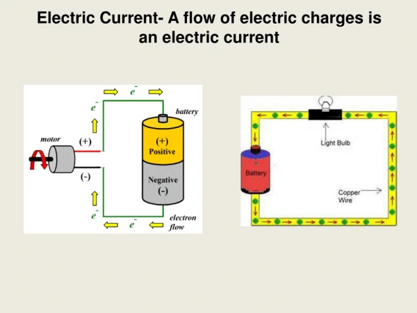
Electrical Components and Circuits Electric current ; the motion of a charge through a medium. Electric units ; the unit of charge (or quantity of electricity) ; C(coulomb) → 0.001111800g of silver ion → silver metal 로 환원시키는데 필요로 하는 전하량 . 1Faraday = 9.649 x 10 4 coulombs

E N D
Electrical Components and Circuits Electric current ; the motion of a charge through a medium. Electric units ; the unit of charge (or quantity of electricity) ; C(coulomb) → 0.001111800g of silver ion → silver metal로 환원시키는데 필요로 하는 전하량. 1Faraday = 9.649 x 10⁴ coulombs 1Faraday ; 107.868g의 은 석출 1g 당량의 원소나 화합물을 석출. ↳ (6.02 x 10²³ charged particle에 대응하는) I = dQ/dt (Q : charge, A : ampere)
2A-1 Laws of Electricity 두 점 사이의 electrical potential (V) ; 공간의 한 점에서 다른 점까지 1개의 전하를 움직이는데 는 일. V ; volt → joule/conlomb (W/Q = V) = (I․R) R ; ohm → R의 단위 Ω(R = ρℓ/A) ↳ ohm's law G ; 저항의 역수(electrical conductance) Ω-1, S I ; Ampere P ; electrical power. joules/sec, W P = dw/dt = V․dQ/dt = V․I P = (I․R)․I = I2R. joule's law
Kirchhoff's Laws Current low ; the algebraic sum of currents around any point in a circuit is zero. Voltage low ; the algebraic sum of the voltages around a closed electrical loop is zero. Direct current ; 전하가 시간에 비례 Alternating current ; 전하가 주기적으로 변화하는 것.
2A-2 Direct-Current Circuits • series circuits • Fig 2-1. a battery, a switch, & three resistors in series.
ⓐ 점 D에서 kirchhoff's law 적용 I4 - I3 = 0 or I4 = I3 at point C. I3 = I2 * the current is the same at all points I = I1 = I2 = I3 = I4 ⓑ Voltage low V - V3 - V2 - V1 = 0 or V = V1 + V2 + V3 by ohm's law V = 1(R1 + R2 + R3) = IReq ∵ Req = R1 + R2 + R3 IR1 = V1 , V2 = IR2 , V3 = IR3
Voltage dividers ; Fig 2-3 a → series connection of resistor ↳ discrete increnents
2) Parallal Circuits Resistor in parallel at point A Kirchhoff's current law I1 + I2 + I3 - I = 0 I = I1 + I2 + I3
Kirchhoff's voltage law I1 = V/R1 V - I1/R1 =0 V= I1R1 I2 = V/R2 V - I2/R2 =0 V = I2R2 I3 = V/R3 V = I3R3 I = I1 + I2 + I3에 위식 代入 V V V V I = --- = --- + --- + --- V1 = V2 = V3 = V Req R1 R2 R3 so that 1 1 1 1 --- = --- + --- + --- Req R1 R2 R3 G=1/R G = G + G + G Parallal resistances create a current divider I1 V/R1 1/R1 G1 R G1 --- = ----- = ----- = --- or I1 = I--- = I--- I V/R 1/R G R1 G
(Ex. 2-1) a) the total resistance b) the current from the battery c) the current present in each of the resistors d) the potential drop across each of the resistors
1 1 1 • ( --- + --- ) = --- • R2 R3 R2,3 • 1 1 1 3 • --- = --- + --- = --- R2,3 = 13.3Ω • R 20 40 40 V 1.5 b) The current ; V = I·R I = --- = ----- = 0.67A R 22.3 c) V = V1 + V2 + V3 V1 = I1R1 = 6.03 I = I2 = I3이므로 9.0 V1 = 15 x ------------ = 6.0V (9.0 + 13.3) 13.3 V2 = V3 = V2,3 = 15 x ------ = 9.0V 22.3 d) R1에서 I1 = I = 0.67G I2 = 9.0/20 = 0.45A I3 = 9.0/40 = 0.22A
2B Alternating current Circuits Alternating voltage and current: 시간에 따라 방향과 크기가 변화하며 똑같은 변화가 계속 반복되는 전압 또는 전류. ;the simplest alternating waveform is sine-wave volt or current Cycle; one complete revolution Frequency(f) [HZ]; time number of cycles per second
2B-1 Sinusoidal Signals The AC: produced by rotation of a coil in a magnetic fiedd. A pure sine wave → 일정한 각속도로 회전 하는(시계방향) IP의 vector로 표시. (여기서 Ip : amplitude.) 주기 t 내에 2π radian 의 속도로 회전 할 때 W = 2π/t = 2πf Any time t에서 instantaneous value → Vpsinwt Vp ; maximum or peak voltage; the amplitude 순간 전류 : ⅰ= Ip sin wt = Ip sin 2πft 순간 전압 : v = Vp sin wt = Vp sin 2πft Out of phase by 90o Phase difference : phase angle(φ) 일반식 ; ⅰ= Ip sin(wt + φ) = Ip sin(2πft + φ) (rms current voltage) ;
DC, AC의 크기비교 ; 두 전류에 의한 저항에서 야기되는 Joule heat DC = the effective value of a sinusoidal, current Report, heating effect of AC is calculated by averaging I2R losses even complete cycle
1 Hz 중의 평균 열손실 = 직류일 때의 ohm손실 square wave ; 파행도 1.00 파고율 1.00 sine wave ; 파행율 = 1.11 파고율 = 1.41 삼각파 ; 파행율 = 1.15 파고율 = 1.73
2B-2 Reactance in Electrical Circuits Reactance - capacitance : capacitor inductance : inductor Use ; ① converting alternating current to DC or the converse ② discriminating among signals of different frequencies or separating ac & dc signals. Capacitors 구성 ; a pair of conductors separated by a thin layer of a dielectric substance
Position 1 Position 2
1) Capacitance ① a momentary current ② current ceases → to be changed ③ switch을 2로 discharge. Capacitor : 전류의 측정可 ① 과 ② 사이에서 switch 껌; 측면 전하가 저장 The quantity of electricity Q → 판 넓이, 모양, 공간, 절연체 의 유전상수에 의해 결정
1 Faraday ; 1 V의 전위치에 의해 양극판에 축적된 전하의 크기가 1 C일 때의 capacitance. μF, PF V = 1/C ∫idt = 1/C∫ Ip sin wt dt = -1/wc Ip cos wt = 1/wc Im sin(wt - π/2) ∵ Vp = 1/wc Ip, V = (1/wc) I 1/wc = Xc → capacitive reactance 단위 Ω Xc = -1/wc V =│Xc│I
2) Inductance Coil에 직류 통과 → 자기작용에 의한 유기전압으로 인해 다른 전류 발생 자기장이 변화 → emf 발생 V = -L(di/dt) - : 전류의 방향과 반대 L : inductance [Henrys] → [H] 1 Henry : 전류변화속도가 one A/1 sec 일 때 1volt의 전압 발생, μH ~ H 범위 V = L(d/dt)(Ip sin wt) = WLIp coowt = WLIp sin(wt + π/2) 전압의 위상이 전류보다 π/2 앞선다. V = wLI 여기서 wL을 inductive reactance라 한다. XL= 2πfL 직류만 통과, 교류 불통 (저주파 chohing coli) 직렬 연결 : L = L1+ L2+ L3
Rate of current & potential changes in an RC circuit By Kirchhoff 의 voltage law Vi = Vc + VR Vi : const Vi = q/C + iR
Rate of Current & Potential Change across RL circuit. RC circuit와 유사한 방법으로 처리 VR = Vi( I - e-tR/L ) VL = Vi e-tR/L L/R : time constant
2B-4 Response of Series RC Circuits to Sinusoidal Inputs Response of series RC & RL circuits to sinusoidal inputs signal (Vs)
At sufficiently high frequencies & capacitance, φ become negligible & e vs are in phase. 1/wC은 저항 R에 비해 무시 可. ↳ 전류가 잘 흐름 At very low frequencies, the phase angle π/2
Voltage, current and phase Relationships for series RL circuit
Capacitive & Inductive Reactance ; impedance Xc = 1/wC = 1/2πfC XL = wL = 2πfL Impedance Z ; 교류회로에서 전압과 전류의 크기의 비(직류회로의 저항에 해당) At, RC circuit Z = √R2 + Xc2 Z = √R2 + XL2 Ip = Vp/Z 저항과 차이점 : ① frequency dependent ② current와 voltage 사이에 phafe diffrence
<Vector diagrams for Reactive Circuits> V가 ⅰ보다 90°늦다. at capacitence V가 ⅰ보다 90°빠르다. at inductance Z = √R2 + (XL - Xc)2 Z = √R2 + Xc2 , φ = -anctan Xc/R Z = √R2 + XL2 , φ = -arctan XL/R Z = √R2 + (XL+ Xc)2 φ = -arctan (XL+ Xc) / R(XL> Xc 인 경우) ex) ① peak current ② voltage drop Z = √(50)2 + (40 - 20)2 = 53.8Ω Ip = 10 v/53.8 = 0.186A Vc = 0.186 x 20 = 3.7V VR = 0.186 x 50 = 9.3V VL = 0.186 x 40 = 7.4V
2B-5 Filters Based on RC Circuits High-pass & Low-Pass Filters RC & RL circuits → low f component를 지나는 동안 high-f signals을 낮추기 위해 filter로 사용 (low pass filter) or 역이 성립. ① RC circuit에서 high-pass filter Vo : across the resistor R
2B-6 The Response of RC Circuits to Pulsed Inputs <Resonant Circuits> impedance Z가 최소 즉 XL = Xc일 때 전류 I = E/Z = E/R ↳ the condition of Resonance resonant frequency fo ; 1/2πfoC = 2πfoL ∵ fo = 1/2π√LC ex) (Vp)i = 15.0 V (peak voltage), L = 100mH, R = 20Ω, C = 1.200μF.
2B-7 Alternating Current, Voltage, and Impedance Measurements Parallel Resonance Filters Xc = XL fo = 1/2π√LC Z of the parallel circuit Z = √R2 + (XLXc/Xc-XL)2 At parallel circuit at resonance → Z는 최대 → maximum voltage drop 生 → tank circuit Behavior of RC Circuits with pulsed inputs RC 회로에 pulse 加 → various form (with of pulse time const) 사이의 관계에 의존 Simple Electrical Measurements Galvanometers → DC의 전류, 저항 측정원리 : the current in duceol motion of a coil suspended in a yixed magnetic yiedd. ⇒ D'arsonval movement or coil. He Ayrton Shunt : to vary the range of a galvanometers p29. 예제 참조☆ measurement of current and voltage.
2C Semiconductors and Semiconductor Devices Semiconductors - Electronic circuits contain one or more nonlinear devices such as transistors, semiconductor diodes, and vacuum or gas-filled tubes. Nonlinear components ; rectification (from ac to dc ) amplitude modulation or frequency modulation vacuum tube → Semiconductor based diodes and transistors → integrated circuits (Tr, R, C & conductor) -Semiconductor 장점 : low cost, low power consumption, small heat generation, long life and compactness.
2C-1 Properties of silicon & germanium semiconductors. • Sufficient thermal agitation occurs at room temp. to liberate an occasional electron from its bonded state, leaving it free to more through the crystal lattice and thus to conduct electricity. • Hole : positively charged region. • -Electron: negatively charged region. • -Hole & electron 의 이동방향 반대. • -Doping of arsenic or antimony (Group Ⅴ) → n type • of indium or gallium (Group Ⅲ) → p type • Positive holes are less mobile them free electrons. • Conductivity of n type >conductivity of p type.
2C-2 . Semiconductor Diodes Pn junction motion → diode is a nonlinear device that has greater conductance in one direction than in another. Figure 2-15 A pn junction diode (c) forward - bias (d) reverse - bias → depletion layer 생성 : conductance 10-6~10-8
Figure 2-16 I - V cures for semiconductor Diodes The voltage at which the sharp increase in current occurs under reverse bias is called the Zener breakdown voltage.
2C-3 Transistors : Amplifying device -Bipolar -Field effect transistor. ① Bipolar Tr. : pnp, npn tr.
The mechanism of amplification with a bipolar transistor. Pnp on ∽ n layer ~ 0.02mm thickness, p>>n layer. (수백배 이상), ∴The concentration of holes in p >> that of electrons in n layer
① P-type emitter junction 에서 hole 생성 ② ①번의 hole 이 very thin n-type base 로 이동 - electron 과 결합 (basecurrentIB유발) ③ 대부분의 hole 은 base를 통해 drift 되어 collector junction 으로 attracting ④ 여기서 power supply로부터 나온 electron 과 combined 되어 전류 흐름 (Ic) The no of current carrying holes is a fixed multiple of the number of electrons supplied by the input base current.
Field Effect Transistors (FET) FET - The insulated gate field effect transistor. →109~1014Ω 의 imput impedence → MOSFET (metal oxide semiconductor FET) n- chanel MOSFET The gate is a cylindrical p-type semiconductor surrounding a center core of n -doped material called the channel. Two isolated n regions are formed in a p-type substrate. 위의 n.p regions 을 silicon dioxide로 insulating