Download
1 / 13
240 likes | 768 Views
1. Crystal Properties and Growth of Semiconductors. Electrical behavior of solids Arrangement of atoms. 1.1. Semiconductor Materials. Electrical conductivity intermediate between metals and insulators. W. t. L. What distinguishes semiconductors? - resistance/resistivity

E N D
1. Crystal Properties and Growth of Semiconductors • Electrical behavior of solids • Arrangement of atoms 1.1. Semiconductor Materials • Electrical conductivity intermediate between • metals and insulators
W t L What distinguishes semiconductors? - resistance/resistivity - crystalline structure The resistance of a bar of material with dimensions L, W, t: Resistivityis: metals: < 10-3-cm insulators: >102-cm semiconductors: 10-3-cm < < 102-cm
Figure 1: Electrical conductivities of some common materials.
*Conductivity of semiconductor material can be varied over orders of magnitude by changes in -temperature -optical excitation -impurity content Periodic table: Column IV Si, Ge Elemental semiconductors III-VCompound semiconductors example:GaAs II-VICompound semiconductors example:CdTe
Binary compounds: GaAs, GaP, GaN, CdTe, InP etc. Ternary compounds: AlGaAs, GaAsP, HgCdTe, etc. Quaternary compounds: InGaAsP, AlGaInAs,etc. Applications: *transistors, integrated circuits (Si) *light emitting diodes (LEDs) (GaAs,GaN, GaP) *lasers (AlGaInAs, InGaAsP, GaAs, AlGaAs) *light detectors(Si, InGaAsP, CdSe, InSb, HgCdTe)
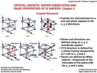
1.2. Crystal Lattices • Solids classified according to atomic arrangement: • Crystalline • Amorphous • Polycrystalline (a) Crystalline (b) Amorphous (c) Polycrystalline
The atoms making up the CRYSTAL are arranged in a periodic fashion called LATTICE. UNIT CELL is a representative of the entire lattice and is generally repeated throughout the structure. PRIMITIVE CELL is the smallest unit cell that can be repeated to form the lattice. • Crystal lattice determines: • Density of solid (mechanical property) • Allowed energy bands of electrons (electrical property).
Cubic Lattices Simple (SC) Body-centered (BCC) Face-centered (FCC) a – lattice constant
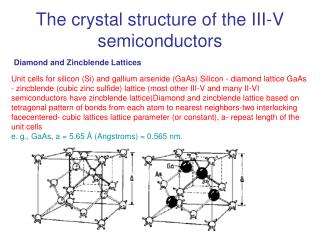
Diamond Lattice Top view Diamond lattice is an FCC plus placing atoms ¼ a, ¼ a, ¼ a (in x, y and z direction) from each atom in the FCC. Construction of a diamond lattice from two interpenetrating FCC sublattices.
*Diamond (zincblende) lattice - typical of most of the commonly used semiconductors. *Characteristic of Si, Ge, III-V compounds. *Possible to vary the composition of alloy by choosing the fraction of numbers of the atoms, par example: AlxGa1-xAs (x % of Al, (1-x)% of Ga) InxGa1-xAsyP1-y
Conclusion • Atomic arrangement in certain planes in crystal is important to many of the mechanical, metallurgical, and chemical properties of the material. • Crystals cleaved along certain atomic planes, resulting in exeptionally planar surfaces • Chemical reactions-etching of a crytal often take place preferentially along certain directions