Download
1 / 24
250 likes | 471 Views
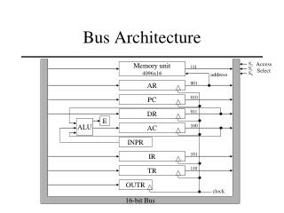
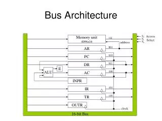
The Bus Architecture of Embedded System. ESE 566 Report 1 LeTian Gu. CoreConnect Bus Architeture. Fig.1 The CoreConnect bus architecture in a SOC. Processor Local Bus . to interface between the processor cores and integrated bus controllers

E N D
The Bus Architecture of Embedded System ESE 566 Report 1 LeTian Gu
CoreConnect Bus Architeture Fig.1 The CoreConnect bus architecture in a SOC
Processor Local Bus • to interface between the processor cores and integrated bus controllers • be developed for use in Core+ASIC and system-on-a-chip (SOC) designs • providing a high bandwidth data path
PLB performances • Decoupled address, read data, and write data buses • Concurrent read and write transfers • Address pipelining • Ability to overlap the bus request • grant protocol with an ongoing transfer
PLB’s flexibility features: • Support multiple masters and slaves • Four priority levels for master requests • Deadlock avoidance • Master driven atomic operations • Byte-enable capability • A sequential burst protocol allowing byte, half-word, word and double-word burst transfers
CONTINUE • Support for 16-, 32- and 64-byte line data transfers • Read word address capability • DMA support for buffered, fly-by transfers • Guarded or unguarded memory transfers • Architecture extendable to 256-bit data buses
Continue • PLB transactions consist of multiphase address and data tenures • A PLB transaction begins when a master drives its address and transfer qualifier signals and requests ownership of the bus during the request phase of the address tenure • Once the PLB arbiter • grants bus ownership the master's address and transfer qualifiers are presented to the slave devices • during the transfer phase
On-Chip Peripheral Bus (OPB) • Peripherals attach to OPB include serial ports, parallel ports, UARTs, GPIO, timers and other low-bandwidth devices • OPB alleviate system performance bottlenecks by reducing capacitive loading on the PLB
CONTINUE • synchronous 32-bit address,data buses • support byte, half-word and word transfers • A sequential address (burst) protocol • Support for multiple OPB bus masters • Bus parking for reduced-latency transfers
Device Control Register (DCR) Bus • Transfer data between the CPU’s general purpose registers and the DCR slave logic’s device control registers
Features of DCR bus • 10-bit address bus and 32-bit data bus • 2-cycle minimum read or write transfers • Handshake supports clocked asynchronous transfers • Slaves may be clocked either faster or slower than master • Distributed multiplexer architecture
A clocking scheme up to 4 GHz • clock skew and jitter becoming a higher percentage of the cycle time. • power-supply fluctuations and cross coupling result • larger die area • diminishing device geometries result in less manufacturing control
jitter reduction • filtering the power supply of clock-tree drivers • shielding of clock wires from signal coupling. to supply noise from logic switching • low-pass RC filter show 5 times reduction in noise amplitude on the filtered supply
Continue • main components are 47 adjustable delay buffers (DB) and a phase-detector (PD) network.(include 46 PD) • test access port (TAP) control the delay adjustment against the primary PD • skew is adjusted to within accumulation error of about 8 ps. In this particular condition, the preadjusted skew is about 64 ps
power saving in the interconnection • Interconnect often dominate the power consumption • On chip, an interconnect comprises a driver, a wire with total capacitance, and a receiver with capacitive load • Off chip, a high-speed interconnect comprises a driver, an interconnect, which normally is a 50- transmission line, and a receiver with a termination resistor and an amplifier
power consumption and voltage swing in an interconnect • One way to reduce the power consumption related to interconnect is to reduce the voltage swing used • an amplifier at the receiver side is needed to restore the swing to its normal value • optimum swing means at which the power consumption used to drive the wire balances the power consumption of the receiver
Total power versus input voltage swing Solid line: case 1. Dashed line: case 2. Upper curves a = 0:25 and lower a = 0:05.
Data for analysis • analysis was held assuming CMOS technology with 0.18-um process and CMOS logical swings. fc=1GHz, Vdd = 1.3V, CL=10pf, Cw=1pf, a represent data activity. 0.25 and 0.05 are used. • Cw of 1pf corresponds to an internal wire of 5–10 mm.
Results of analysis • The power consumption of the wire is 85uW and 0.42 mW at full swing for a =0.05 and a= 0.25 • optimum voltage swings exists in a wide range of situations, and depends on operating frequency, data activities, and different cases for generating the reduced voltage • Case1.optimum swings of the order of 100 to 400 mVpower savings of the order of 10X • Csae 2. optimumvoltage swings of 60 to 120 mV savings are limited to 3X to 8X
Conclusions • More devices will involve into interconnect • Interconnect bus trace often dominate the power consumption • resistant transmission line theory should be used in analysis in higher frequency • robust interconnect architecture will efficiently realize complex system-on-a-chip design and component reuse