Download
1 / 39
580 likes | 2.62k Views
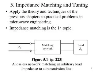
jX 1. jB 2. Y L. Impedance Matching with Lumped Elements. jX 1. Z L. jB 2. Single-Stub Matching. Load impedance . Input admittance=S. Series Stub. Voltage minimum. Input impedance=1/S. Double Stub Matching Network. a. b. Y L. jB 2. jB 1. b. a. x=1. Y L. P open circuit .

E N D
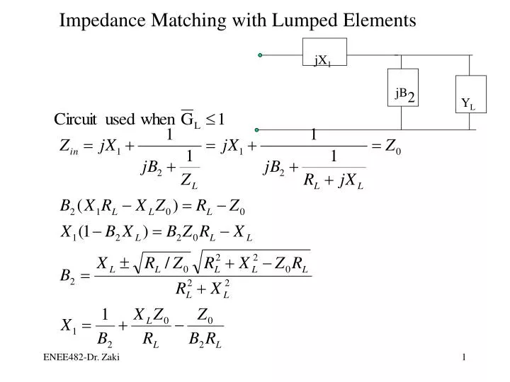
jX1 jB2 YL Impedance Matching with Lumped Elements
jX1 ZL jB2
Single-Stub Matching Load impedance Input admittance=S
Series Stub Voltage minimum Input impedance=1/S
Double Stub Matching Network a b YL jB2 jB1 b a
x=1 YL Popen circuit Pshort circuit r=1 0 r=0.5 Real part of Refl. Coeff. Smith Chart x=-1
x=1 P2 YL G1=1 Popen circuit Pshort circuit r=1 0 r=0.5 Real part of Refl. Coeff. P3 Smith Chart x=-1 Rotate the the G=1 circle through an angle -f The intersection of G=1 and the GL circle determine The point P2
x=1 YL Popen circuit Pshort circuit r=1 0 r=0.5 Real part of Refl. Coeff. x=-1 Smith Chart The shaded range is for the load impedance which cannot be matched when d=1/8 wavelength
Quarter-Wave Transformers ZC=Z0 ZL ZC=Z1 l /4
r Dq rm 3p/2 p/2 qm p q Bandwidth characteristic for a single Section quarter wave transformer
1 Z2 G3 G1 ZL Z1 G2 G T12 T21 Theory of Small Reflection q
T21 1 G1 Multiple reflection of waves for a circuit with two reflection junctions
Approximate Theory for Multi-Section Quarter Wave Transformers q q q G3 ZL Z2 Z1 Z0 ZN A multi-section quarter-wave transformer
Example Z3 ZL Z2 Z1 Z0 Design a three section binomial transformer to match a 50 Ohms load to a 100 Ohms line. Calculate the bandwidth For max reflection =.05 over the passband.
rm qm p/2 q p- qm Chebyshev Transformer
Example Design a two section Chebyshev transformer (two sections) to Match a line of load impedance =2. The maximum tolerance Value of r is 0.05.
Design of Complex Impedance Termination Amplifier Zc Zc Input Matching network ZL Output Matching network Zs Microwave amplifier circuit
l l jB1 = ZL ZL G=1 Zc Stub Transmission Line Matching Network jX1 jX2 jB2 jB1 ZL ZL G=1 G=1 Alternative Matching Networks
l/l = 0.0626 l/l = 0.4375 j1 Generator 1 Y’in YL G=2 ZL= 0.4-j0.2 2 Load Y”in G=1 -j1 Design Procedure for the Matching Network with Shunt Stub
Z22-Z12 Z11-Z12 ZT ZS ZL ZL Z12 VS Voc ML Zin A T matching network Thevenin equivalent network
Zg Z0 Vg ZL Impedance Transformation and Matching Review of Transmission Lines and Smith Chart Z=L Z=0 Finite Transmission Line terminated with load impedance L
Standing wave ration (SWR) S: Smith Chart:
Imaginary part of Refl. Coeff. x=1 Popen circuit Pshort circuit r=1 0 r=0.5 Real part of Refl. Coeff. x=-1 Smith Chart
Review of Transmission Lines and Smith Chart Zg Z0 Z=L Vg Z=0 ZL L Finite Transmission Line terminated with load impedance