Download
1 / 12
130 likes | 196 Views
Explore thermal oxidation and CVD techniques for silicon dioxide and silicon nitride deposition in ICs and MEMS fabrication processes. Discover the growth rates, materials properties, and deposition methods for electronic materials used in semiconductor manufacturing.

E N D
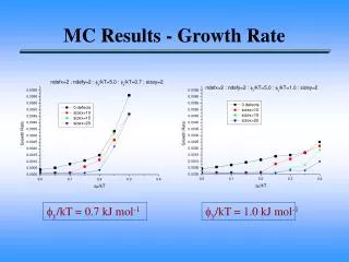
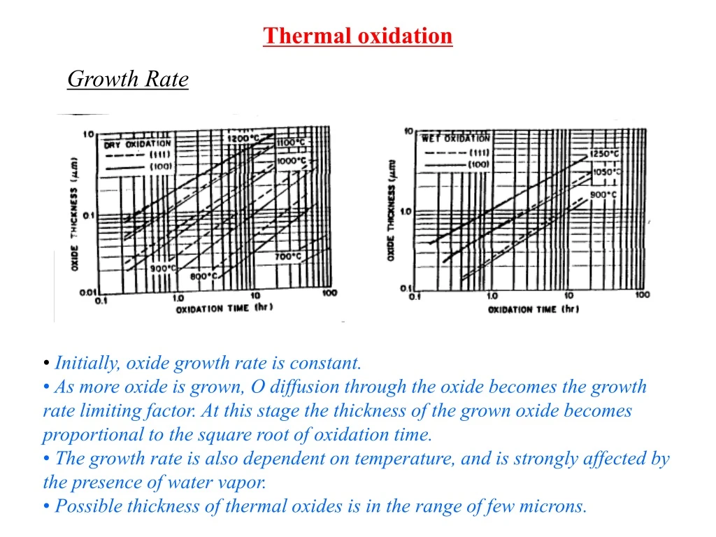
Thermal oxidation Growth Rate • Initially, oxide growth rate is constant. • As more oxide is grown, O diffusion through the oxide becomes the growth rate limiting factor. At this stage the thickness of the grown oxide becomes proportional to the square root of oxidation time. • The growth rate is also dependent on temperature, and is strongly affected by the presence of water vapor. • Possible thickness of thermal oxides is in the range of few microns.
The basic structural unit of thermal oxide is a Si atom surrounded tetrahedrally by four oxygen atoms. • The Si-O and O-O internuclear distances are 1.6 Å and 2.27 Å, respectively. • SiO2 or silica has several crystalline structures (the dominant one is quartz), and an amorphous structure. • Amorphous oxide has a density of ~ 2.2 gm/cm3, whereas quartz has a density of ~ 2.7 gm/cm3. • Thermally grown oxides are usually amorphous.
ELECTRONIC MATERIALS • To fabricate ICs and MEMS many different kinds of bulk materials and thin films are used. • The bulk materials are predominantly semiconductors. • The most important semiconductor for ICs and MEMS is Si. • Thin films in ICs and MEMS are classified into four groups : Thin films thermal SiO2 dielectrics Poly-Si metals deposited SiO2 deposited Si3N4
Dielectric And Polycrystalline Silicon Film Deposition : Low Pressure Chemical Vapor Deposition (LPCVD) • The furnace is similar to the thermal oxidation furnace, with the two exceptions : (1) pressure of deposition typically between 100 and 50 mTorr, and (2) non-uniform temperature over the length of the furnace tube. • The low pressure is to allow surface catalyzed reaction of otherwise highly reactive (in some cases explosive) gases. • The temperature variation is to compensate for depletion of the reactants. • Typical LPCVD parameters are (i) pressure ; 0.2 to 2.0 Torr, (ii) gas flow ; 1 to 10 cm/s, and (iii) temperature ; 300 to 900 °C.
CVD of Silicon Dioxide • Low-temperature (300 to 500 °C) deposition : • SiH4 + O2 SiO2 + 2H2 • The low temperature of the deposition makes it suitable when films must be deposited over a layer of Al. • Intermediate-temperature (500 to 800 °C) deposition : • The oxide is formed by decomposing tetraethylorthosilicate (TEOS), Si(OC2H5)4. TEOS decomposes as follows : • Si(OC2H5)4 SiO2 + by-products • The high temperature of deposition makes it inappropriate for film deposition on Al, however it is used for depositing insulating films on poly-Si. • High-temperature (900 °C) deposition : • SiCl2H2 + 2N2O SiO2 + 2N2 + 2HCl 450 °C 700 °C 900 °C
ELECTRONIC MATERIALS • To fabricate ICs and MEMS many different kinds of bulk materials and thin films are used. • The bulk materials are predominantly semiconductors. • The most important semiconductor for ICs and MEMS is Si. • Thin films in ICs and MEMS are classified into four groups : Thin films thermal SiO2 dielectrics Poly-Si metals deposited SiO2 deposited Si3N4
CVD of Silicon Nitride • In the LPCVD process, dichlorosilane and ammonia react at reduced pressure to deposit silicon nitride at 700 °C ≤ T ≤ 800 °C : • Good film uniformity, and high wafer throughput (i. e., number of wafers processed per hour) are advantages of the process. • Silicon nitride deposited by LPCVD is an amorphous dielectric containing up to ~ 8% hydrogen. • The nitride film has a very high tensile stress of approximately 1010 dynes/cm2 which is ~ 10 times that of silicon dioxide. • The resistivity of the nitride at room temperature is ~ 1016Wcm, its dielectric constant is 6, and its dielectric strength is 107 V/cm.
Polysilicon Deposition • It is deposited from silane in a low-pressure reactor operated between 600 and 650 °C. • The reaction :
LPCVD Materials, Gases, and Deposition Temperatures • Because of deposition temperature, most metals can not be placed in LPCVD furnaces.