Download
1 / 29
290 likes | 413 Views
Multi-ported Memories for FPGAs via XOR. Eric LaForest, Ming Liu, Emma Rapati, and Greg Steffan ECE, University of Toronto. Multi-Ported Memories (MPM). MPM: Memory with more than 2 ports Many uses: register files queues/buffers FPGA BRAMs: have only 2 ports Building MPMs:

E N D
Multi-ported Memories for FPGAs via XOR Eric LaForest, Ming Liu, Emma Rapati, and Greg Steffan ECE, University of Toronto
Multi-Ported Memories (MPM) • MPM: Memory with more than 2 ports • Many uses: • register files • queues/buffers • FPGA BRAMs: • have only 2 ports • Building MPMs: • multiple BRAMs • logic elements (ALMs/LEs) • clever combinations … … Write Ports Read Ports
Example: 2W/2R MPM How can we build this?
2W/2R: Pure-ALMs/LEs Scales very poorly with memory depth
1W/2R: Replicated BRAMS X M0 R0 W0 M1 R1 Fairly efficient Only one write port
2W/2R Banked BRAMs X M0 W0 R0 M1 R1 W1 Fragmented data Multiple write ports
2W/2R “Multipumping” W0 R0 M0 R1 W1 Divides clock speed No fragmentation
Review:The Live Value Table (LVT) Approach(FPGA’10) Efficient Multi-Ported Memories for FPGAs, Eric LaForest and J. Gregory Steffan, International Symposium on Field-Programmable Gate Arrays, Monterey, CA, February, 2010.
LVT-Based MPM Bank for two write ports, replicate to provide read ports LVT: remembers which bank has most recently- written value Muxes select bank to read from LVT
LVT-Based MPM Many ALMs! Significant Multiplexing! Punchline: LVT is a big freq win, but...
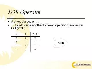
XOR • XOR basics: A ⊕ 0 = A B ⊕ B = 0 • Implication: A ⊕ B ⊕ B = A Can we exploit XOR to build better MPMs? Intuition: avoid LVT-table, multiplexing
2W/2R XOR Design R0 Goal: a read is only an XOR operation
2W/2R XOR Design A⊕OLD A⊕OLD⊕OLD R0 =A A⊕OLD OLD OLD Focus on one location for now
2W/2R XOR Design A A⊕OLD W0 A⊕OLD OLD R0 OLD XOR new value with old value
2W/2R XOR Design W0 R0 Support multiple locations, two write ports
2W/2R XOR Design A W0 A⊕OLD1 OLD2 R0 B W1 OLD1 B⊕OLD2 Most-recently-written bank holds new value XOR old(s)
2W/2R XOR Design W0 R0 W1 R1 Add support for second read port---done! (almost)
2W/2R XOR Design A W0 TOCK R0 W1 TICK R1 Writing requires reading: hence 2 cycles to write! Solution: need pipelining to avoid stalling
2W/2R XOR Design A W0 Read? R0 W1 TICK R1 What if read a location one cycle after written? Solution: bypass with forwarding logic
Methodology Use Quartus 10.0 to target Stratix IV Favor speed over area, optimize Average over 10 seeds to get Fmax Measure area as Total Equivalent Area (TEA) Expresses area in a single unit (ALMs) 1 M9K == 28.7ALMs ** Measure a large design space Depth: 32-8192 memory locations Ports: 2W/4R, 4W/8R, 8W/16R ** H. Wong, J. Rose and V. Betz, "Comparing FPGA vs. Custom CMOS and the Impact on Processor Microarchitecture," ACM Int. Symp.on FPGAs, 2011
Example Layout: 8192-deep 2W/4R XOR LVT Significant resource diversity!
2W/4R Faster 8192 XOR: 15% faster, 2x smaller CAD anomaly Smaller (log) LVT better for small designs, XOR better for large
Navigating the Design Space (2W/4R) Which is best? That depends...
Summary 4W/8R 2W/4R 8W/16R • Use LVT when: • want to minimize BRAMs • building <= 128 depth • else use XOR, i.e. when: • >= 256 & spare BRAMS
Conclusions • Use LVT when • building up to 128-entry designs • you want to minimize BRAM usage • Use XOR when • building 256-entry or larger designs • you want to minimize ALM usage • Interesting Library/Generator? • help the designer automatically navigate this space • Further work • Exploring “true-dual-port” mode, stalls, power • Results on other vendor’s FPGAs