Download
1 / 5
50 likes | 199 Views
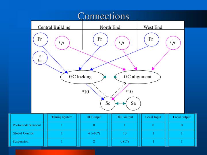
Timing System. DOL input. DOL output. Local Input. Local output. Photodiode Readout. 1. 0. 1. 0. 0. Central Building. North End. West End. Pr. Pr. Pr. Qr. Qr. Qr. Global Control. 1. 4 (+10?). 10. 1. 1. Pr Inj. Suspension. 1. 2. 0 (1?). 1. 1. GC. lo. cking.

E N D
Timing System DOL input DOL output Local Input Local output Photodiode Readout 1 0 1 0 0 Central Building North End West End Pr Pr Pr Qr Qr Qr Global Control 1 4 (+10?) 10 1 1 Pr Inj. Suspension 1 2 0 (1?) 1 1 GC lo cking GC alignment *10 *10 S c S a Connections
Block Diagram FastEthernet VME Console PC104PlusCPU Module FastEthernet PCI2VMEBridge PCI2PCIBridge PC104PlusCPU Module Console PCI 4 Link Port PCI2LBBridge Dual Port Memory 2 DSP#1 DSP#3 2 DSP#5 DOL Timing Serial link 4 3 DSP Local Bus Front Panel LB2VSBBridge FlashMemory DSP#2 DSP#4 DSP#6 Serial link 4 Front Panel VSB Link Port
8 8 8 8 DOL/Timing mezzanine Clk Synchronization 32bits GPS words FPGA CONNECTOR DSP External clk Misc Timing Interface Serial port DOL Optical receiver Link ports Optical Interface DOL Optical receiver DOL Optical receiver PCI target interface Optical transmitter DOL Optical transmitter PCI connector
Connector P1 FPGA VME interface (config and control) and interface between the mezzanine board and the 10 optical transmitters P2 DOL DOL DOL DOL DOL DOL DOL DOL DOL DOL Optical transmitter Optical transmitter Optical transmitter Optical transmitter Optical transmitter Optical transmitter Optical transmitter Optical transmitter Optical transmitter Optical transmitter DOL Extension (Global Control)
14.8 cm 4 cm DSP7 x 14 DOL& Timing PC104Plus9.5 x 9 5.5 cm VME Connectors