Download
1 / 13
130 likes | 318 Views
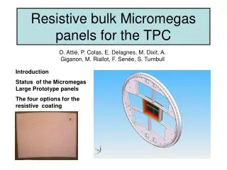
Resistive bulk Micromegas panels for the TPC. D. Attié, P. Colas, E. Delagnes, M. Dixit, A. Giganon, M. Riallot, F. Senée, S. Turnbull. Introduction Status of the Micromegas Large Prototype panels The four options for the resistive coating. Introduction.

E N D
Resistive bulk Micromegas panels for the TPC D. Attié, P. Colas, E. Delagnes, M. Dixit, A. Giganon, M. Riallot, F. Senée, S. Turnbull Introduction Status of the Micromegas Large Prototype panels The four options for the resistive coating
Introduction Avalanche size in Micromegas: 12-14 microns. => no natural charge sharing To obtain the best possible (diffusion-limited) resolution down to z=0, need to share the charge between pads One solution (M. Dixit et al.) : use a continuous RC circuit to spread the charge. In addition, by spreading the charge of sparks over space and time, they limit the effect of discharges. On the other hand, bulk technique is mandatory to avoid dead areas and provide robustness => Make compatible these two techniques (r) r (mm) P. Colas - Micromegas resistive panels
The panels Two routings have been done One in Saclay with 6 layers (delivered early June) One at CERN with 4 layers (to be delivered next week) HV P. Colas - Micromegas resistive panels
One of the 3 routing layers of the Saclay PCB P. Colas - Micromegas resistive panels
Mechanical support of the electronics The AFTER-based (T2K) electronics has been fully commissioned. The shielding and supporting structure for the cards has been assembled The software for analysing pedestals (pad monitor) is up and running. (without shielding, the pedestal rms was already 4 ADC counts). P. Colas - Micromegas resistive panels
Mechanical support of the electronics P. Colas - Micromegas resistive panels
The problematic of resistive layers Resistive layers are difficult matter to work with. They are often non-uniform, non-ohmic (the resistance depends on the voltage applied), they evolve with time (slow arrangements of dipoles, in the case of milled conductive solids in a resin). In general the conductivity is governed by addition of tiny quantities of a dopant, so very difficult to master. In addition, the market (mostly US) is rather closed, as high resistivity materials are used in radar furtiveness, or in high value applications as photovoltaics. Simulations are on-going to optimise parameters (Analog Artist, E. Delagnes and S. Turnbull). gas resistive insulator 25 AFTER Preamps P. Colas - Micromegas resistive panels
The 4 techniques. 1) resistively-covered kapton This will be tried by Madhu Dixit on a Saclay panel. It is the following of the sucessful AlSi CERMET, but on kapton instead of mylar (Mylar would not stand the conditions for making bulks. Sheets of diamond-like carbon (1012W/sq) have been sent to Rui de Oliveira at CERN for tests. By doping 10 MOhm/sq should be possible Also in the process to get an Yttrium-Al garnet. P. Colas - Micromegas resistive panels
The 4 techniques. 2) carbon-loaded kapton This was the first technique used. It was abandoned since the resistivity was too low (0.5 MOhm/sq) and higher resistivities were not available. Rui de Oliveira managed to get a roll from Dupont, nominally 10 MW/sq (measured 2.7 MW/sq at 250 V) 2 prototypes will be made at CERN and this process will be tried on one of the CERN panels. P. Colas - Micromegas resistive panels
The 4 techniques. 3) prepreg + screen-printing This has been tried at CERN. 2 prototypes of 10x10 cm (2 and 8 MOhm/sq) have been tried at Saclay. There is not clear evidence that they are spark protected. Even one of the detector has been damaged by the HV during the test. Still such a layer will be applied to a CERN panel. P. Colas - Micromegas resistive panels
The 4 techniques. 4) thin-layer deposition An agreement between CEA Saclay and Neuchatel University has been set up to study the feasability and attempt to make a prototype from amorphous silicon deposition. The first phase was to check that the NELCO 7000 PCB does not outgas, and perform tests of adherence and uniformity. These tests are in progress. 250°C deposition 180°C deposition 230°C deposition At 230 and 250 °C the resistive layer does not adhere to copper. At 180 it adheres but peals off with time. P. Colas - Micromegas resistive panels
The 4 techniques. 4) thin-layer deposition Orders of magnitude calculation : We obtained good results with 75 micron insulator, er = 2.5, Rsurf = 1 MW/sq To keep the same RC, with aSiH as ‘insulator’ and dopped aSiH (or another resistive deposition) on top, we calculate the resistivity of the top layer assuming 5 micron for the lower layer (er = 11) and 0.5 micron for the top layer. This implies a surface resistivity of 15 kW/sq, and a bulk resistivity of 0.75 W.cm. It might be difficult to obtain such a low bulk resistivity by simple doping. P. Colas - Micromegas resistive panels
Conclusion The basics mechanics, electronics and DAQ software are ready for the LP test. The bulk technique for applying the mesh is well established at CERN. There is still some work for developing and optimising the resistive layer. A lot of work is going on at CERN, Saclay, Carleton and Neuchatel to this end. P. Colas - Micromegas resistive panels