Download
1 / 37
370 likes | 559 Views
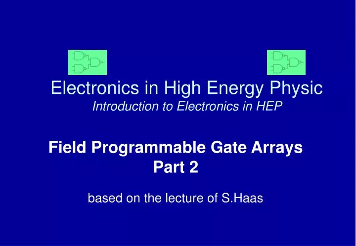
Electronics in High Energy Physic Introduction to Electronics in HEP. Field Programmable Gate Arrays Part 2 based on the lecture of S.Haas. Part 2 VHDL Introduction Examples Design Flow Entry Methods Simulation Synthesis Place & Route IP Cores CERN Tools & Support. Part 1

E N D
Electronics in High Energy PhysicIntroduction to Electronics in HEP Field Programmable Gate ArraysPart 2 based on the lecture of S.Haas
Part 2 VHDL Introduction Examples Design Flow Entry Methods Simulation Synthesis Place & Route IP Cores CERN Tools & Support Part 1 Programmable Logic CPLD FPGA Architecture Examples Features Vendors and Devices coffee break Outline
VHDL Language • Hardware Description Language (HDL) • High-level language for to model, simulate, and synthesize digital circuits and systems. • History • 1980: US Department of Defense Very High Speed Integrated Circuit program (VHSIC) • 1987: Institute of Electrical and Electronics Engineers ratifies IEEE Standard 1076 (VHDL’87) • 1993: VHDL language was revised and updated • Verilog is the other major HDL • Syntax similar to C language • At CERN VHDL is mostly used for FPGA design • Many tools accept both Verilog and VHDL
Terminology • Behavioral modeling • Describes the functionality of a component/system • For the purpose of simulation and synthesis • Structural modeling • A component is described by the interconnection of lower level components/primitives • For the purpose of synthesis and simulation • Synthesis: • Translating the HDL code into a circuit, which is then optimized • Register Transfer Level (RTL): • Type of behavioral model used for instance for synthesis
Digital Circuits and VHDL Primitives • Most digital systems can be described based on a few basic circuit elements: • Combinational Logic Gates: • NOT, OR, AND • Flip Flop • Latch • Tri-state Buffer • Each circuit primitive can be described in VHDL and used as the basis for describing more complex circuits.
C X D AND E W F NOR Digital Circuit Primitives • Combinational Logic Gates: NOT, OR, AND • Flip Flop/Latch • Tri-state Buffer • Logic gates can be modeled using concurrent signal assignments: Z <= not A; Y <= A or B; X <= C and D; W <= E nor F; U <= B nand D; V <= C xor F; • It is possible to design circuits from logic gates in this way • For design entry it is preferable to use other VHDL structures that allow circuit descriptions at a higher level of abstraction
Combinatorial Logic: Decoder Example: 2-to-4 decoder Z(3) entity decoder is port ( A : in std_logic_vector(1 downto 0); Z : out std_logic_vector(3 downto 0) ); end entity decoder; architecture when_else of decoder is begin Z <= "0001" when A = "00" else "0010" when A = "01" else "0100" when A = "10" else "1000" when A = "11" else "XXXX"; end architecture when_else; A(1) Z(2) Interface A(0) Z(1) Z(0) Functionality
a b y c d S(1) S(0) 4-to-1 Multiplexer entity mux is port ( a, b, c, d: in std_logic; s: in std_logic_vector(1 downto 0); y: out std_logic); end entity mux; architecture mux1 of mux is begin process (a, b, c, d, s) begin case s is when "00“ => y <= a; when "01" => y <= b; when "10" => y <= c; when "11" => y <= d; end case; end process; end architecture mux1;
Sequential Logic: D-Flip Flop architecture rtl of D_FF is begin process (Clock, Reset) is begin if Reset = ‘1’ then Q <= ‘0’; if rising_edge(Clock) then Q <= D; end if; end process; end architecture rtl; Flip-flop D Q D Q Clock R Reset
This example is not explicit on the primitives that are to be used to construct the circuit. The “+” operator is used to indicate the increment operation. Binary Counter entity counter is generic (n : integer := 4); port ( clk : in std_logic; reset: in std_logic; count: out std_logic_vector(n-1 downto 0) ); end entity counter; use ieee.numeric_std.all; architecture binary of counter is begin process (clk, reset) variable cnt : unsigned(n-1 downto 0); begin if reset = '1' then -- async reset cnt := (others => '0'); elsif rising_edge(clk) then cnt := cnt + 1; end if; count <= std_logic_vector(cnt); end process; end architecture binary;
clk curr_state State Transition Logic Output Logic R State Machine If a trigger signal is received, will stretch it to 2 cycles and wait for accept signal entity trigger is port ( clk, reset: in std_logic; trigger, accept : in std_logic; active: out std_logic); end entity trigger; architecture rtl of trigger is type state_type is (s0, s1, s2); signal cur_state, next_state: state_type; begin registers: process (clk, reset) begin if (reset='1') then cur_state <= s0; elsif rising_edge(clk) then cur_state <= next_state; end if; end process; trigger accept reset
clk curr_state State Transition Logic Output Logic R State Machine (cont.) process (cur_state, trigger, accept) is begin case cur_state is when s0 => active <= '0'; if (trigger = '1') then next_state <= s1; else next_state <= s0; end if; when s1 => active <= '1'; next_state <= s2; when s2 => active <= '1'; if (accept = '1') then next_state <= s0; else next_state <= s2; end if; end case; end process; S0 S1 trigger S2 accept
FPGA Design Flow Design Specification Design Entry/RTL Coding Behavioral or Structural Description of Design • RTL Simulation • Functional Simulation • Verify Logic Model & Data Flow • (No Timing Delays) LE • Synthesis • Translate Design into Device Specific Primitives • Optimization to Meet Required Area & Performance Constraints MEM I/O • Place & Route • Map Primitives to Specific Locations inside • Target Technology with Reference to Area & • Performance Constraints • Specify Routing Resources to Be Used
FPGA Design Flow Timing Analysis - Verify Performance Specifications Were Met - Static Timing Analysis tclk Gate Level Simulation -Timing Simulation - Verify Design Will Work in Target Technology Program & Test - Program & Test Device on Board
Text-based: emacs VHDL-mode • Special mode for editing VHDL source files in emacs • Features: • Syntax colouring • Automatic completions • Automatic indentation • Templates for all VHDL constructs • Launching external VHDL compiler
Design Entry: Visual Elite HDL • HDL design and verification environment • Features: • Enables graphical and text-based design entry methods • Design verification using built-in or external simulator • Generation of synthesizable VHDL or Verilog code appropriate for the selected synthesis tool • Design unit types: • Block Diagram • HDL Code • State Diagram • Flowchart • Truth Table
Block Diagram • Hierarchical design methods: • top-down • bottom-up • Contents of a block can be any type of design unit • Top-level block diagram: • Partitioning of the design • Connections between the underlying HDL design units
State Diagram • “Bubble” diagram • States • Conditions • Transitions • Outputs • Useful for developing control modules
Truth Table • Normally used to describe combinatorial logic • Can also be used for sequential circuits (e.g. state machines)
Design Entry Simulation Synthesis Place & Route Simulation Program device & test Design Cycle: Simulation • Functional simulation: • simulate independent of FPGA type • may postpone selection • no timing • Timing simulation: • simulate after place and routing • detailed timing
Example of simulation waveforms. Test vectors are normally defined in a VHDL unit (testbench) Simulation Results
Design Entry Simulation Synthesis Place & Route Simulation Program device & test RTL Synthesis • Input is RTL code • Compilation & translation • Generates technology independent netlist • RTL schematic (HDL code analysis) • Technology mapping • Mapping to technology specific structures: • Look-up tables (LUT) • Registers • RAM/ROM • DSP blocks • Other device specific components/features • Logic optimization • Implementation analysis (technology view)
Technology Mapping Example 6-bit binary counter Altera Stratix device
Design Entry Simulation Synthesis Place & Route Simulation Program device & test Design Cycle: Place and Route • FPGA fitter • Tools supplied by the FPGA vendor • Specific for each FPGA device architecture • Functions • Place-and-route • Constraints editor • Backannotated netlist for timing simulation • Configuration bitstream
Example: Altera Quartus II • Fully integrated design tool • Multiple design entry methods • Text-based: VHDL, Verilog, AHDL • Built-in schematics editor • Logic synthesis • Place & route • Simulation • Timing & power analysis • Create netlist for timing simulation • Device programming • Xilinx ISE has similar features
Macros & IP Cores • Macros: • Generic pre-made design blocks: • e.g. PLL, FIFOs, DDR I/O, Multiply-accumulate, etc. • Accelerate design entry and verification • Pre-optimized for FPGA vendor architecture • Provided at no cost by the FPGA vendor to optimize performance • Instantiate block in the design: • Makes HDL code technology dependent • IP cores: • More complex blocks: PCI-X interface, CPU, etc. • Some are provided by the FPGA vendor • IP cores from third party suppliers cost money • Evaluation before buying usually possible
System On a Programmable Chip • Many ready-made blocks for free • RAM/FIFO • UART • Can buy ready-made parts, just like IC's: IP Cores • PCI interface • Processors (8051-style up to RISC/ARM processors) • FPGA's with extra dedicated hardware built-in • Gigabit serialiser • high-end processor with RAM • Handle different I/O standards • LVDS, LVPECL, LVCMOS, LVTTL, PCI, PCI-X • Programmable slew-rate, termination resistors
Tools available at CERN • Design entry: • FPGA vendor tools • Visual HDL • Cadence ConceptHDL • Simulation • Cadence NCsim • Synthesis • Synplify (Synplify) • Leonardo (Mentor) • FPGA fitter built-in • FPGA vendor tools: • Altera, Xilinx, Actel, Lattice
IP cores: PCI & PCI-X Master/Target for Altera Altera NIOS-II Processor soft core DDR SDRAM controller DSP cores for Altera: FFT, NCO, FIR 10/100/1000 Ethernet MAC If you need an IP core contact IT-PS or the DUG Tools for implementing DSP systems in FPGAs: Xilinx system generator for DSP Altera DSP builder & evaluation kit Altera NIOS-II evaluation kit Programming cables for FPGAs are available for short-term loan Tool usage: Windows PC tools can be installed from: \\dsy-srv4\caeprogs CAE Sun cluster: login to dsy-srv Tools available at CERN (cont.)
CERN Support for FPGA Development • IT/PS – Tool Support Send e-mail to: Dig-Electronics-Cae.Support@cern.ch Direct contact: Serge Brobecker, John Evans http://cern.ch/product-support/electronicscae.html • Other resources: • Mailing list for electronics designers at CERN: cern-electronics@cern.ch • Digital CAE User's Group (DUG): http://wwwinfo.cern.ch/ce/dc/DUG/DUG_home.html • Technical Training: • Visual HDL course • Introduction to VHDL & using the ncvhdl simulator from Cadence http://cern.ch/humanresources/Training/tech/electronics/te_elec.asp
Bibliography • Acknowledgements: • E. van der Bij (CERN), J. Christiansen (CERN) • Further reading: • FPGA vendor sites: http://www.altera.com http://www.xilinx.com … • P. Alfke (Xilinx), “Field Programmable Gate Arrays in 2004”, Proceedings of LECC’2004. • M. Zwolinski, “Digital System Design with VHDL - 2nd Ed.”, Prentice-Hall, 2000, (Chap. 4 & 6)