Download
1 / 30
410 likes | 821 Views
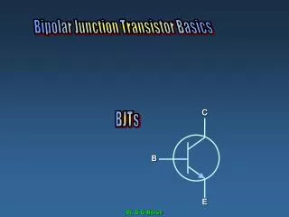
Chapter 4 DC Biasing–BJTs. Biasing. Biasing: T he DC voltages applied to a transistor in order to turn it on so that it can amplify the AC signal. Operating Point. The DC input establishes an operating or quiescent point called the Q-point . The Three States of Operation.

E N D
Biasing Biasing: The DC voltages applied to a transistor in order to turn it on so that it can amplify the AC signal.
Operating Point The DC input establishes an operating or quiescent point called the Q-point.
The Three States of Operation • Active or Linear Region Operation • Base–Emitter junction is forward biased • Base–Collector junction is reverse biased • Cutoff Region Operation • Base–Emitter junction is reverse biased • Saturation Region Operation • Base–Emitter junction is forward biased • Base–Collector junction is forward biased
DC Biasing Circuits • Fixed-bias circuit • Emitter-stabilized bias circuit • Collector-emitter loop • Voltage divider bias circuit • DC bias with voltage feedback
The Base-Emitter Loop From Kirchhoff’s voltage law: +VCC – IBRB – VBE = 0 Solving for base current:
Collector-Emitter Loop Collector current: From Kirchhoff’s voltage law:
Saturation When the transistor is operating in saturation, current through the transistor is at its maximum possible value.
ICsat IC = VCC / RC VCE = 0 V VCEcutoff VCE = VCC IC = 0 mA where the value of RB sets the value of IB that sets the values of VCE and IC Load Line Analysis The end points of the load line are: The Q-point is the operating point:
Emitter-Stabilized Bias Circuit Adding a resistor (RE) to the emitter circuit stabilizes the bias circuit.
Base-Emitter Loop From Kirchhoff’s voltage law: Since IE = (b + 1)IB: Solving for IB:
Collector-Emitter Loop From Kirchhoff’s voltage law: Since IE IC: Also:
Improved Biased Stability Stabilityrefers to a circuit condition in which the currents and voltages will remain fairly constant over a wide range of temperatures and transistor Beta () values. Adding RE to the emitter improves the stability of a transistor.
Saturation Level The endpoints can be determined from the load line. VCEcutoff: ICsat:
Voltage Divider Bias This is a very stable bias circuit. The currents and voltages are nearly independent ofany variations in .
Approximate Analysis Where IB << I1 and I1 I2 : Where bRE> 10R2: From Kirchhoff’s voltage law:
Transistor Saturation Level Voltage Divider Bias Analysis • Load Line Analysis • Cutoff: Saturation:
DC Bias with Voltage Feedback Another way to improve the stability of a bias circuit is to add a feedback path from collector to base. In this bias circuit the Q-point is only slightly dependent on the transistor beta, .
Base-Emitter Loop From Kirchhoff’s voltage law: Where IB << IC: Knowing IC = IB and IE IC, the loop equation becomes: Solving for IB:
Collector-Emitter Loop Applying Kirchoff’s voltage law: IE + VCE + I’CRC – VCC = 0 Since IC IC and IC = IB: IC(RC + RE) + VCE – VCC =0 Solving for VCE: VCE = VCC – IC(RC + RE)
Transistor Saturation Level • Load Line Analysis • Cutoff: Saturation: Base-Emitter Bias Analysis
Transistor Switching Networks Transistors with only the DC source applied can be used as electronic switches.
Switching Circuit Calculations Saturation current: To ensure saturation: Emitter-collector resistance at saturation and cutoff:
Switching Time Transistor switching times:
Troubleshooting Hints • Approximate voltages • VBE .7 V for silicon transistors • VCE 25% to 75% of VCC • Test for opens and shorts with an ohmmeter. • Test the solder joints. • Test the transistor with a transistor tester or a curve tracer. • Note that the load or the next stage affects the transistor operation.
PNP Transistors The analysis for pnp transistor biasing circuits is the same as that for npn transistor circuits. The only difference is that the currents are flowing in the opposite direction.