Download
1 / 16
170 likes | 310 Views
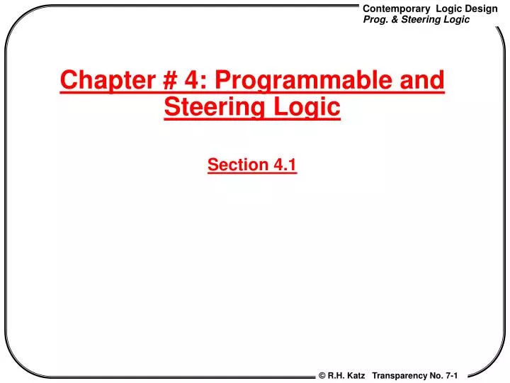
Chapter # 4: Programmable and Steering Logic Section 4.1. PALs and PLAs. Pre-fabricated building block of many AND/OR gates (or NOR, NAND) "Personalized" by making or breaking connections among the gates. Programmable Array Block Diagram for Sum of Products Form.

E N D
PALs and PLAs Pre-fabricated building block of many AND/OR gates (or NOR, NAND) "Personalized" by making or breaking connections among the gates Programmable Array Block Diagram for Sum of Products Form
PLA -- Programmable Logic Array PAL -- Programmable Array Logic A typical TTL field-PLA might have 16 inputs, 48 product terms, 8 outputs -- 24 data pins Equivalent -- forty-eight 16-input AND gates and eight 48-input OR gates. 12 data-pin SSI package gives four 2-input gate PALs and PLAs
PALs and PLAs Key to Success: Shared Product Terms Equations F0 = A + B' C' F1 = A C' + A B F2 = B' C' + A B F3 = B' C + A Example: Input Side: 1 = asserted in term 0 = negated in term - = does not participate Personality Matrix Output Side: 1 = term connected to output 0 = no connection to output Need a 3-input, 5-product term, 4-output --- PLA device
PALs and PLAs Example Continued All possible connections are available before programming A B C F0 F1 F2 F3
Programmer -- hardware device which personalizes the array Programming process depends on the particular IC Frequent technique -- places fuses between all possible inputs to a gate and the gate itself. Programmer hardware breaks the connections by placing a high current across selected fuses PALs and PLAs Example Continued
PALs and PLAs Example Continued A B C Unwanted connections are "blown" AB B’C AC’ F0 = A + B' C' F1 = A C' + A B F2 = B' C' + A B F3 = B' C + A B’C’ A Note: some array structures work by making connections rather than breaking them F0 F1 F2 F3
F1 = A B C F2 = A + B + C F3 = A B C = A’ + B’ + C’ F4 = A + B + C = A’B’C’ F5 = A B C = A’B’C + A’BC’ + AB’C’ + ABC F6 = A B C = ABC’ + A’BC + AB’C + A’B’C’ PALs and PLAs Design Example A B C Function Generator of 3 inputs: A, B, C The circuit should implement the logic functions AND, OR, NAND, NOR, XOR, XNOR ABC A B C A’ B’ C’ A’B’C’ A’B’C A’BC’ AB’C’ ABC’ A’BC AB’C F1 F2 F3 F4 F5 F6
PALs and PLAs Alternative representation for high fan-in structures 4-input, 4-output, 4 product terms Short-hand notation so we don't have to draw all the wires! A B C D Notation for implementing F0 = A B + A' B' F1 = C D' + C' D AB + A’B’ CD’ + C’D
PALs and PLAs What is difference between Programmable Array Logic (PAL) and Programmable Logic Array (PLA)? PAL concept — implemented by Monolithic Memories. Programmable AND array but connections between product terms and specific OR gates are hardwire (constrained topology of the OR Array). A given column of the OR array has access to only a subset of the possible product terms PLA concept — generalized topologies in AND and OR planes. Can be programmed in any way. PLA can take advantage of shared product terms. PAL cannot. PLA is slower because of the relative resistance of programmable and hardwired connections.
PALs and PLAs Design Example: BCD to Gray Code Converter Truth Table K-maps Minimized Functions: W = A + B D + B C X = B C' Y = B + C Z = A'B'C'D + B C D + A D' + B' C D'
PALs and PLAs A B C D No shared product terms, PAL implementation is best. Programmed PAL: 4 inputs, 16 Programmable ANDS 4 4-input ORS 4 outputs A BD BC 0 BC’ 0 0 0 B C 0 0 A B C D BCD AD’ B’CD’ 4 product terms per each OR gate W X Y Z
PALs and PLAs Code Converter Discrete Gate Implementation 5 SSI Packages vs. 1 PLA/PAL Package!
PALs and PLAs Another Example: Magnitude Comparator What is more efficient, a PLA or PAL?
PALs and PLAs Another Example: Magnitude Comparator (cont’d) Since AC’ and A’C are used twice, (shared), a PLA-based implementation is better than a PAL.. A B C D ABCD ABCD ABCD ABCD AC AC BD BD ABD BCD ABC BCD EQ NE LT GT