Download
1 / 5
50 likes | 62 Views
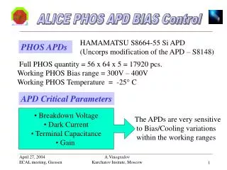
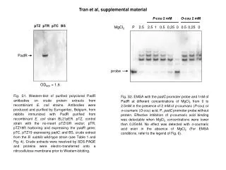
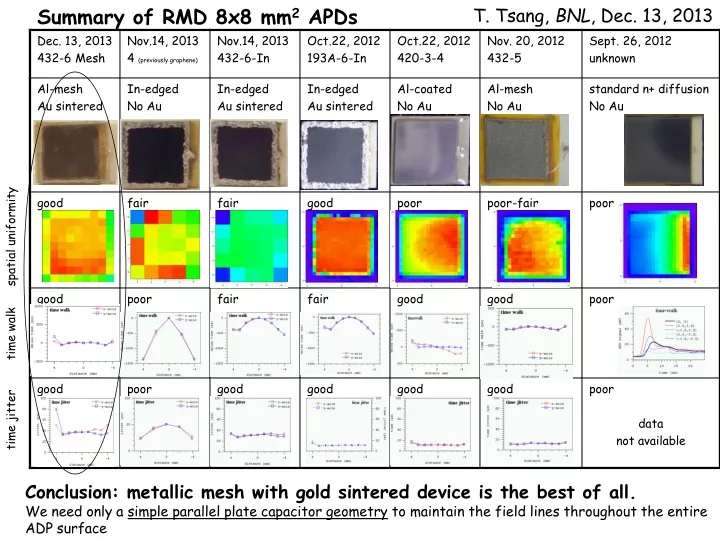
Study on the spatial uniformity, time walk, and time jitter of 8x8 mm2 APDs using metallic mesh with gold sintered device, indicating it as the best option. The research demonstrates the simplicity of a parallel plate capacitor geometry to maintain field lines across the APD surface.

E N D
Summary of RMD 8x8 mm2 APDs T. Tsang, BNL, Dec. 13, 2013 spatial uniformity time walk time jitter Conclusion: metallic mesh with gold sintered device is the best of all. We need only a simple parallel plate capacitor geometry to maintain the field lines throughout the entire ADP surface
Dec. 13, 2013 APD 8x8 mm2 Al-mesh, Au sintered, s/n 432-6 APD bias at -1.85 kV 980 nm Vcsel, ~1 ns pulse, 1 kHz ~1 MIP equivalent photons on APD (accounted for the transmission of mesh + etc ~50%) Circuit diagram no amplifier direct APD output 1-MIP at -1.85 kV 256 ave. Mesh APD signal output ground -HV marking on the back
Dec. 13, 2013 APD 8x8 mm2 Al-mesh, Au sintered, s/n 432-6 -1.85 kV ~1 MIP spatial response map ← + y-position ← + x-position
Dec. 13, 2013 APD 8x8 mm2 Al-mesh, Au sintered, s/n 432-6 -1.85 kV ~1 MIP time walk map ← + y-position ← + x-position
Dec. 13, 2013 APD 8x8 mm2 Al-mesh, Au sintered, s/n 432-6 -1.85 kV ~1 MIP time jitter map ← + y-position ← + x-position 1-MIP 8x8mm2σ(0,0)=36.5 ps ~1 MIP σIRF=7.3 ps