Download
1 / 21
210 likes | 248 Views
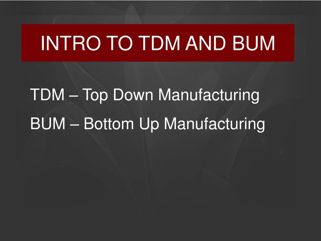
INTRO TO TDM AND BUM. TDM – Top Down Manufacturing BUM – Bottom Up Manufacturing. TOP DOWN MANUFACTURING. Materials modified Cutting, drilling, milling Machinery used Many steps needed Primary method in integrated circuits industry. BOTTOM UP MANUFACTURING.

E N D
INTRO TO TDM AND BUM TDM – Top Down Manufacturing BUM – Bottom Up Manufacturing
TOP DOWN MANUFACTURING • Materials modified • Cutting, drilling, milling • Machinery used • Many steps needed • Primary method in integrated circuits industry
BOTTOM UP MANUFACTURING • Similar to way nature builds objects • Self-assembly • Atomic force microscope • The future of nano-manufacturing?
MOORE’S LAW • Integrated circuits (ICs) are electronic circuits on a single piece of silicon • Circuits on ICs are made from many transistors • Since 1965 trend is for the number of transistors per integrated circuit to double every two years • In 1965 there were 30 transistors per chip • Today, more than 1 billion transistors per chip
TDM IN SEMICONDUCTOR MANUFACTURING • Transistors are semiconductor devices • Transistors connected together form circuits • Integrated circuits consists of many transistors • Many ICs built simultaneously on silicon wafers • Transistors are built first, then interconnected • ICs are built in a chip fab
TDM IN SEMICONDUCTOR MANUFACTURING • ICs are built layer by layer • Process steps include: • Wafer photolithography ion implant • Deposition metallization • Steps repeated many times for each IC
PHOTOLITHOGRAPHY • Mask is high quality glass • Mask has areas marked to block transmission of light • One mask for every layer of the IC • Photoresist covers IC • Ultraviolet light shines through mask onto photoresist • Photoresist affected by light
PHOTOLITHOGRAPHY • Photolithography defines transistor size • Part of process is to reduce image on mask • Transistors made of several features • Feature size defines how small transistors are • Smallest feature size currently is 45nm
PROBLEM WITH TDM • TDM processing reaching physical limits • Difficult to reduce mask images to smaller and smaller levels • Requires shorter wave length light (X-rays) • Requires more sophisticated optical systems to reduce images • This are expensive and technically challenging
Bottom Up Manufacturing • Possible way to continue Moore’s Law progress • Build features one atom at a time • Use forces of nature to accomplish this • No machining necessary • Requires proper environmental conditions
AFM • Atomic force microscope • Can image atoms • Can move atoms • Forces between atom and ATM tip interact • Measurement of forces used to produce image of atom or to manipulate atoms • IBM logo made from xenon atoms in 1990
SELF-ASSEMBLY • Self-assembly occurs naturally • Smaller features are created • Smaller features combine to produce larger features • Combinations occur until macro structure is built
SELF-ASSEMBLY IN SOAP • Soap bubbles consist od soap molecules and water molecules • Soap molecule ends react differently with water • Hydrophili end links with water easily • Hydrophobic end will not link with water • Monolayers form to create bubble wall • Wall is soap-water-soap
SELF-ASSEMBLY IN SOAP • http://nanopedia.case.edu/NWPage.php?page=soap.bubbles • http://www.nanooze.org/english/articles/article14_selfassembly.html
PROPERTIES OF NANOSTRUCTURES • Objects at the nano-scale exhibit unique properties • Properties may not exist at larger scales • Color • Light reflection • Order
COLOR PROPERTIES OF SOAP • http://www.exploratorium.edu/ronh/bubbles/bubble_colors.html • http://www.exploratorium.edu/ronh/bubbles/bubble_meets_bubble.html