Download
1 / 29
290 likes | 308 Views
This study investigates various quantum-mechanical effects in Trigate SOI MOSFETs, including dopant fluctuation, quantum confinement, intersubband scattering, and variation of threshold voltage.

E N D
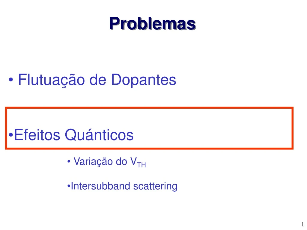
Problemas • Flutuação de Dopantes • Efeitos Quánticos • Variação do VTH • Intersubband scattering
tsi Wsi Wsi=tsi=20 nm / FMS=0V / VG= 0.0V / VG2=0V / Na=5x1017 cm-3 / T=300K Electron concentration (Poisson) Electron concentration (Poisson+Schrödinger )
tsi Wsi Wsi=tsi=20 nm / FMS=0V / VG= 1.5V / VG2=0V / Na=5x1017 cm-3 / T=300K Electron concentration (Poisson) Electron concentration (Poisson+Schrödinger )
tsi Wsi Wsi=tsi= 5 nm / FMS=0V / VG=0.0V / VG2=0V / Na=5x1017 cm-3 / T=300K Electron concentration (Poisson+Schrödinger ) Electron concentration (Poisson)
tsi Wsi Wsi=tsi= 5 nm / FMS=0V / VG=1.5V / VG2=0V / Na=5x1017 cm-3 / T=300K Electron concentration (Poisson) Electron concentration (Poisson+Schrödinger )
2D Simulation (Quantum) Electron concentration
Problemas • Flutuação de Dopantes • Efeitos Quánticos • Variação do VTH • Intersubband scattering
First (lowest) subband energy level and Threshold voltage "Quantum-Mechanical Effects in Trigate SOI MOSFETs", J.P. Colinge, J. C. Alderman , W. Xiong, and C. R. Cleavelin, IEEE Transactions on Electron Devices, Vol. 53, no 5, pp. 1131-1136, 2006
Corrente de Dreno Poisson equation only (P) or Poisson+Schrödinger solver (P+S) "Quantum-Mechanical Effects in Trigate SOI MOSFETs", J.P. Colinge, J. C. Alderman , W. Xiong, and C. R. Cleavelin, IEEE Transactions on Electron Devices, Vol. 53, no 5, pp. 1131-1136, 2006
Problemas • Flutuação de Dopantes • Efeitos Quánticos • Variação do VTH • Intersubband scattering
Inter-Subband Scattering (2D GaAs)
Efeitos Quánticos: Inter-subband scattering At low temperature
Efeitos Quánticos: Inter-subband scattering At room temperature !
Experimental Results FinFET/Tri-Gate Technology • 150nm Buried oxide • 65 nm top silicon layer thickness (HFIN) • gate dielectric = 2.3 nm HfSiON on 1 nm SiO2 • midgap metal gate: • 5 nm TiN layer + 100nm thick polysilicon capping • 1 x1015cm-3 channel concentration
Threshold Voltage - MuGFET For MuGFETs Devices (*): Top gate Side gate The influence of side gates are considerably higher than the top gate for Wfin = 20 nm (almost double gate) Side gate *T. Poiroux et al., Microelectronics Engineering, 80, 378 (2005).
Threshold Voltage - MuGFET For MuGFETs Devices (*): Workfunction difference Between the gate and silicon film *T. Poiroux et al., Microelectronics Engineering, 80, 378 (2005).
Threshold Voltage - MuGFET For MuGFETs Devices: Potential f in the channel
Threshold Voltage - MuGFET For MuGFETs Devices: variation of the minimum energy in the conduction band Confinement induced by the quantum well WFIN = 20 nm *T. Poiroux et al., Microelectronics Engineering, 80, 378 (2005).
Threshold Voltage - MuGFET For MuGFETs Devices: Therefore the last term can be neglected due to the Wfin used in this study has 20 nm Confinement induced by the quantum well WFIN = 20 nm
When WFin decreases Better control of the back channel by side walls gm ramp disappears WFin Vth [6] T. Poiroux et al., Micr. Eng., vol. 80, p. 378, 2005. WFin Sidewalls conduction gmmax reduction is due to the electron mobility degradation in sidewall (110) crystal orientation with respect to the (100) plane
Triple-Gate nFET Strain Technology Strain gm,max Vth
Devices Characteristics – TiN Thickness Study Metal Gate - TiN IMEC/Belgium: Gate dielectric : 1 nm SiO2 chemical oxide 2.3 nm MOCVD HfSiO toxb = 150nm Hfin = 65nm Na = 1x1015 cm-3 n type MuGFETs 10 fins Wfin = 2, 1, 0.5, 0.2, 0.17m Wfin,eff = Wfin - 0.13mm L = 10m Metal Gate – TiN 2nm (64 ALD cycles) 5nm (160 ALD cycles) 10nm (320 ALD cycles) *I. Ferain et al., ESSDERC, p. 202-205, 2008.
TiN Thickness Influence on gm *Rodrigues M, Martino JA, Collaert N, Mercha A, Simoen E, Claeys C (2009)EuroSOI 2009 Back interface accumulated (Fully depleted) to see GIFBE VT increases Thinner TiN metal gate IG VT decreases VFB eWF Thinner TiN reduces slightly the onset of GIFBE
Devices Characteristics – Gate Stack • n type MuGFETs • Wfin = 2m • 10 fins • L = 10m • toxb = 145nm • Hfin = 65nm • Na = 1x1015 cm-3 IMEC/Belgium: *VLSI Symp. Dig. Techn. Papers, p. 14 (2008)- IMEC process Poly-Si Poly-Si Poly-Si Poly-Si Poly-Si Poly-Si Poly-Si 3nm 4 nm 4 nm 5 nm PE-ALD TiN 1 nm TiN 1 nm 0.5 nm 5nm 2nm 1 nm 1 nm 0.5 nm Dy2O3 Cap Layer HfSiO HfSiO HfSiO HfSiO HfSiO HfSiO 2.3nm HfSiO HfSiO HfSiO SiO2 SiO2 SiO2 SiO2 SiO2 SiO2 SiO2 1 nm RTO (IL) SiO2 REF(1) (2) (3) (4) (5)
Gate Stack Influence on gm (*) *Martino JA, et al (2009), SOI Symposium, ECS Transactions. VT (eWF) GIFBE (higher VGF) ( IG)
FinFET/Tri-Gate Technology (High NA) (*) *Andrade MGC, Martino JA (2008), Solid-State Electronics, 52, 1877–1883.
FinFET/Tri-Gate Technology (High NA) Higher NA - three peaks are observed. • VT,TC : Top Corners • VT,BC : Bottom Corners • VT,SG VT,TG :Sidewall and Top surfaces at the same time
CONCLUSÕES Para seguir a Lei de Moore é necessário: • Uso de isolantes de porta com alta constante dielétrica e/ou uso de Múltiplas Portas (FinFET) • Incrementar a corrente (Silício tensionado, SiGe, Ge, Múltiplas Portas (FinFET)). • Modificar a estrutura do MOSFET para melhorar o acoplamento eletrostático: • MOS conv.SOI Múltiplas Portas (FinFET)
Agradecimentos • Jean-Pierre Colinge • Alunos de Mestrado e Doutorado da EPUSP. • Colegas Professores e Doutores da USP, FEI e UNICAMP. • FAPESP: Projeto Temático • CNPq – INCT-NAMITEC : Prof. Jacobus Swart