Download

1 / 8
0 likes | 6 Views
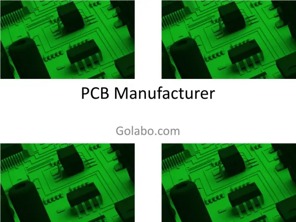
High Quality PCB Co., Limited is a leading PCB(Printed Circuit Board) Manufacturer in China since 1995. Dedicated to technology innovation, being engaged in IC Substrates, High-Density Interconnect PCB, Multi-layer PCB, Rigid Flexible PCB, Flexible and radiofrequency PCB.

E N D
facebook.gif twitter1.gif Pinterest_-_Black_Circle.png WELCOME WELCOME TO TO EFPCB.COM EFPCB.COM
IC Substrate: The Base for Integrated Circuit Packaging IC Substrate: The Base for Integrated Circuit Packaging Laminate substrates, lead frames, bonding wire, encapsulating materials, underfill, die- attach materials, WLP (Wafer-Level Packaging) dielectrics, and WLP plating chemicals are among the most common materials used in integrated circuit packaging. These materials are used to shield and link IC chips to external devices such as printed circuit boards (PCBs), as well as to provide thermal control and support. Read our full blog CLICK CLICK.
Get Into the Deep Insights of Semiconductor Test Board Get Into the Deep Insights of Semiconductor Test Board Semiconductor test boards, often called probe cards or test fixtures, are critical equipment in the semiconductor industry for testing and verifying integrated circuits (ICs) and other semiconductor devices. These boards allow you to electrically connect the devices under test (DUTs) to test equipment such as automated test equipment (ATE) and semiconductor test systems. Check more information about our product CLICK CLICK.
Probe Card PCB is A Significant Aspect of Semiconductor Wafer Test System Probe Card PCB is A Significant Aspect of Semiconductor Wafer Test System In general, the probe card is considered disposable, and maintenance is essential to ensure its performance and usefulness. Overload and the deposition of debris from the wafer's binding material on the probe's tips or probe needles can cause resistance to increase and hinder correct readings. Read our full blog for more CLICK CLICK.
The Importance and Standard of Via on PAD Technology for PCB The Importance and Standard of Via on PAD Technology for PCB in high-speed digital circuits, in order to ensure the integrity of the signal, it is necessary to strictly control the impedance of the signal. Through the design of the Via on PAD, the grounding via can be introduced at a specific position to realize the reference plane switching of the signal, so as to adjust the impedance of the signal and meet the requirements of high-speed signal transmission. Get more information check our blog CLICK CLICK.
Our Organization Our Organization Our Milestones Our Milestones
facebook.gif twitter1.gif Pinterest_-_Black_Circle.png