Download
1 / 77
770 likes | 979 Views
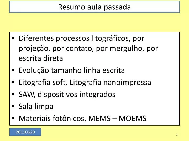
Resumo aula passada. Diferentes processos litográficos, por projeção, por contato, por mergulho, por escrita direta Evolução tamanho linha escrita Litografia soft . Litografia nanoimpressa SAW, dispositivos integrados Sala limpa Materiais fotônicos, MEMS – MOEMS. 20110620.

E N D
Resumo aula passada • Diferentes processos litográficos, por projeção, por contato, por mergulho, por escrita direta • Evolução tamanho linha escrita • Litografia soft. Litografia nanoimpressa • SAW, dispositivos integrados • Sala limpa • Materiais fotônicos, MEMS – MOEMS 20110620
Cristais Fotônicos Elétrons de um lado e fótons do outro lado, junção de fóton + eletrônico (fotônico) Temos elétrons em sólidos e fótons em......materiais fotônicos
Referencias • Fundamentals of Photonics (SALEH AND TEICH · Fundamentals of Photonics, Second Edition. ISBN: 978-0-471-35832-9 ) • Ch. 9: Fiber Optics • Photonic Crystals: Molding the Flow of Light(ISBN: 978-0-691-12456-8) • J. D. Joannopoulos • Photonic crystal tutorials • Steven G. Johnson • http://ab-initio.mit.edu/photons/tutorial/ • MIT Photonic Bands Software • Free program for computing photonic crystal band structures • http://ab-initio.mit.edu/wiki/index.php/MIT_Photonic_Bands
Em Cristal Sólido elétrons potencial periódico banda de energia defeitos: estados dentro da banda proibida Cristais fotônicos Analogia entre cristal sólido e cristal fotônico. • Em Cristal Fotônico • fótons • modulaçãoda constante dielétrica • Banda de energia fotônica = photonic band gap (PBG) • defeitos: estados dentro da banda com direcionalidade bem definida • Analogias • portadores • estrutura • bandas • defeitos Yablonovitch, PRL 58 (1987) 2059; John, PRL 58 (1987) 2486
For the total number Nof atoms in a solid (1023 cm–3), N energy levelssplit apart within a width E. Leads to a band of energiesfor each initial atomic energy level (e.g. 1s energy band for 1s energy level). Band Theory: “Bound” Electron Approach Solid of N atoms Two atoms Six atoms Electrons must occupy different energies due to Pauli Exclusion principle.
Filtro de Fabry-Perot C_MEMS http://www.npphotonics.com/files/article/OEG20030324S0088.htm
O seguinte é um seminário dado porSteven G. Johnson, MIT Applied Mathematics
From electrons to photons: Quantum-inspired modeling in nanophotonics Steven G. Johnson, MIT Applied Mathematics
strange waveguides Nano-photonicmedia (l-scale) & microcavities [B. Norris, UMN] [Assefa & Kolodziejski, MIT] 3d structures [Mangan, Corning] synthetic materials optical phenomena hollow-core fibers
1887 1987 Photonic Crystals periodic electromagnetic media can have a band gap: optical “insulators”
Cristal fotônico 1D e1 e2 e1 e2 e1 e2 e1 e2 e1 e2 e1 e2 1887 e(x) = e(x+a) 1 - D a p e r i o d i c i n o n e d i r e c t i o n
Elétron numa rede periódica 1D Elétron num ambiente livre Solução:
Elétron numa rede periódica – aproximação por poço retangular periódico Mostra a existência de banda proibida, imposta por condições de contorno
Simulation of Band Gap Structures of 1D Photonic Crystal • Journal of the Korean Physical Society, Vol. 52, February 2008, pp. S71S74
dielectric spheres, diamond lattice photon frequency wavevector Electronic and Photonic Crystals atoms in diamond structure Periodic Medium Bloch waves: Band Diagram electron energy wavevector interacting: hard problem non-interacting: easy problem
Electronic & Photonic Modelling Electronic Photonic • strongly interacting —tricky approximations • non-interacting (or weakly), —simple approximations (finite resolution) —any desired accuracy • lengthscale dependent (from Planck’s h) • scale-invariant —e.g. size 10 10 Option 1: Numerical “experiments” — discretize time & space … go Option 2: Map possible states & interactions using symmetries and conservation laws: band diagram
+ constraint eigen-state eigen-operator eigen-value Fun with Math First task: get rid of this mess 0 dielectric function e(x) = n2(x)
Electronic & Photonic Eigenproblems Electronic Photonic simple linear eigenproblem (for linear materials) nonlinear eigenproblem (V depends on e density ||2) —many well-known computational techniques Hermitian = real E & w, … Periodicity = Bloch’s theorem…
A 2d Model System dielectric “atom” e=12 (e.g. Si) square lattice, period a a a E TM H
Periodic Eigenproblems if eigen-operator is periodic, then Bloch-Floquet theorem applies: can choose: planewave periodic “envelope” Corollary 1: k is conserved, i.e.no scattering of Bloch wave Corollary 2: given by finite unit cell, so w are discrete wn(k)
Solving the Maxwell Eigenproblem Finite celldiscrete eigenvalues wn Want to solve for wn(k), & plot vs. “all” k for “all” n, constraint: where: H(x,y) ei(kx – wt) 1 Limit range ofk: irreducibleBrillouin zone 2 Limit degrees of freedom: expand H in finitebasis 3 Efficiently solve eigenproblem: iterative methods
ky kx Solving the Maxwell Eigenproblem: 1 Limit range ofk: irreducible Brillouin zone 1 —Bloch’s theorem: solutions are periodic in k M first Brillouin zone = minimum |k| “primitive cell” X G irreducible Brillouin zone: reduced by symmetry Limit degrees of freedom: expand H in finite basis 2 Efficiently solve eigenproblem: iterative methods 3
Solving the Maxwell Eigenproblem: 2a Limit range ofk: irreducible Brillouin zone 1 Limit degrees of freedom: expand H in finite basis (N) 2 solve: finite matrix problem: Efficiently solve eigenproblem: iterative methods 3
Solving the Maxwell Eigenproblem: 2b Limit range ofk: irreducible Brillouin zone 1 Limit degrees of freedom: expand H in finite basis 2 — must satisfy constraint: Planewave (FFT) basis Finite-element basis constraint, boundary conditions: Nédélec elements [ Nédélec, Numerische Math. 35, 315 (1980) ] constraint: nonuniform mesh, more arbitrary boundaries, complex code & mesh, O(N) uniform “grid,” periodic boundaries, simple code, O(N log N) [ figure: Peyrilloux et al., J. Lightwave Tech. 21, 536 (2003) ] Efficiently solve eigenproblem: iterative methods 3
Solving the Maxwell Eigenproblem: 3a Limit range ofk: irreducible Brillouin zone 1 Limit degrees of freedom: expand H in finite basis 2 Efficiently solve eigenproblem: iterative methods 3 Slow way: compute A & B, ask LAPACK for eigenvalues — requires O(N2) storage, O(N3) time Faster way: — start with initial guess eigenvector h0 — iteratively improve — O(Np) storage, ~O(Np2) time for p eigenvectors (psmallest eigenvalues)
Solving the Maxwell Eigenproblem: 3b Limit range ofk: irreducible Brillouin zone 1 Limit degrees of freedom: expand H in finite basis 2 Efficiently solve eigenproblem: iterative methods 3 Many iterative methods: — Arnoldi, Lanczos, Davidson, Jacobi-Davidson, …, Rayleigh-quotient minimization
Solving the Maxwell Eigenproblem: 3c Limit range ofk: irreducible Brillouin zone 1 Limit degrees of freedom: expand H in finite basis 2 Efficiently solve eigenproblem: iterative methods 3 Many iterative methods: — Arnoldi, Lanczos, Davidson, Jacobi-Davidson, …, Rayleigh-quotient minimization for Hermitian matrices, smallest eigenvalue w0minimizes: minimize by preconditioned conjugate-gradient(or…) “variational theorem”
Band Diagram of 2d Model System(radius 0.2a rods, e=12) a frequencyw(2πc/a) = a / l irreducible Brillouin zone G G X M M E gap for n > ~1.75:1 TM X G H
Preconditioned conjugate-gradient: minimize (h + a d) — d is (approximate A-1) [f + (stuff)] The Iteration Scheme is Important (minimizing function of 104–108+ variables!) Steepest-descent: minimize (h + a f) over a … repeat Conjugate-gradient: minimize (h + a d) — d is f+ (stuff): conjugate to previous search dirs Preconditioned steepest descent: minimize (h + a d) — d = (approximate A-1) f ~ Newton’s method
The Iteration Scheme is Important (minimizing function of ~40,000 variables) no preconditioning % error preconditioned conjugate-gradient no conjugate-gradient # iterations
E|| is continuous E is discontinuous (D = eE is continuous) Any single scalare fails: (mean D) ≠ (anye) (mean E) Use a tensore: E|| E The Boundary Conditions are Tricky e?
The e-averaging is Important backwards averaging correct averaging changes order of convergence from ∆x to ∆x2 no averaging % error tensor averaging (similar effects in other E&M numerics & analyses) resolution (pixels/period)
Gap, Schmap? a frequencyw G G X M But, what can we do with the gap?
Intentional “defects” are good microcavities waveguides (“wires”)
(Same computation, with supercell = many primitive cells) Intentional “defects” in 2d
Microcavity Blues For cavities (point defects) frequency-domain has its drawbacks: • Best methods compute lowest-w bands, but Nd supercells have Nd modes below the cavity mode — expensive • Best methods are for Hermitian operators, but losses requires non-Hermitian
Time-Domain Eigensolvers(finite-difference time-domain = FDTD) Simulate Maxwell’s equations on a discrete grid, + absorbing boundaries (leakage loss) • Excite with broad-spectrum dipole ( ) source Dw Response is many sharp peaks, one peak per mode signal processing complexwn [ Mandelshtam, J. Chem. Phys.107, 6756 (1997) ] decay rate in time gives loss
Signal Processing is Tricky signal processing complexwn ? a common approach: least-squares fit of spectrum fit to: FFT Decaying signal (t) Lorentzian peak (w)
There is a better way, which gets complex w to > 10 digits Fits and Uncertainty problem: have to run long enough to completely decay actual signal portion Portion of decaying signal (t) Unresolved Lorentzian peak (w)
There is a better way, which gets complex w for both peaks to > 10 digits Unreliability of Fitting Process Resolving two overlapping peaks is near-impossible 6-parameter nonlinear fit (too many local minima to converge reliably) sum of two peaks w = 1+0.033i w = 1.03+0.025i Sum of two Lorentzian peaks (w)
Idea: pretend y(t) is autocorrelation of a quantum system: time-∆t evolution-operator: say: Quantum-inspired signal processing (NMR spectroscopy):Filter-Diagonalization Method (FDM) [ Mandelshtam, J. Chem. Phys.107, 6756 (1997) ] Given time series yn, write: …find complex amplitudes ak & frequencies wk by a simple linear-algebra problem!
…expand U in basis of |(n∆t)>: Umn given by yn’s — just diagonalize known matrix! Filter-Diagonalization Method (FDM) [ Mandelshtam, J. Chem. Phys.107, 6756 (1997) ] We want to diagonalize U: eigenvalues of U are eiw∆t
Filter-Diagonalization Summary [ Mandelshtam, J. Chem. Phys.107, 6756 (1997) ] Umn given by yn’s — just diagonalize known matrix! A few omitted steps: —Generalized eigenvalue problem (basis not orthogonal) —Filter yn’s (Fourier transform): small bandwidth = smaller matrix (less singular) • resolves many peaks at once • # peaks not knowna priori • resolve overlapping peaks • resolution >> Fourier uncertainty
Do try this at home Bloch-mode eigensolver: http://ab-initio.mit.edu/mpb/ Filter-diagonalization: http://ab-initio.mit.edu/harminv/ Photonic-crystal tutorials(+ THIS TALK): http://ab-initio.mit.edu/ /photons/tutorial/
A “Defective” Lecture Photonic Crystals:Periodic Surprises in Electromagnetism Steven G. Johnson MIT
a band diagram Bloch form: w k Hermitian –> complete, orthogonal, variational theorem, etc. The Story So Far… Waves in periodic media can have: • propagation with no scattering (conserved k) • photonic band gaps (with proper e function) Eigenproblem gives simple insight:
backwards slope: negative refraction dw/dk 0: slow light (e.g. DFB lasers) synthetic medium for propagation strong curvature: super-prisms, … (+ negative refraction) Properties of Bulk Crystals by Bloch’s theorem band diagram (dispersion relation) (cartoon) photonic band gap conserved frequencyw conserved wavevectork
divergent dispersion (i.e. curvature): Superprisms [Kosaka, PRB58, R10096 (1998).] negative group-velocity or negative curvature (“eff. mass”): Negative refraction, Super-lensing Applications of Bulk Crystals using near-band-edge effects Zero group-velocity dw/dk: distributed feedback (DFB) lasers [ C. Luo et al., Appl. Phys. Lett.81, 2352 (2002) ]
Those Clever Experimentalists Photonic Crystals:Periodic Surprises in Electromagnetism Steven G. Johnson MIT Fabrication of Three-Dimensional Crystals
The Mother of (almost) All Bandgaps (primitive) Recipe for a complete gap: fcc = most-spherical Brillouin zone + diamond “bonds” = lowest (two) bands can concentrate in lines The diamond lattice: fcc (face-centered-cubic) with two “atoms” per unit cell a Image: http://cst-www.nrl.navy.mil/lattice/struk/a4.html