Download
1 / 15
150 likes | 309 Views
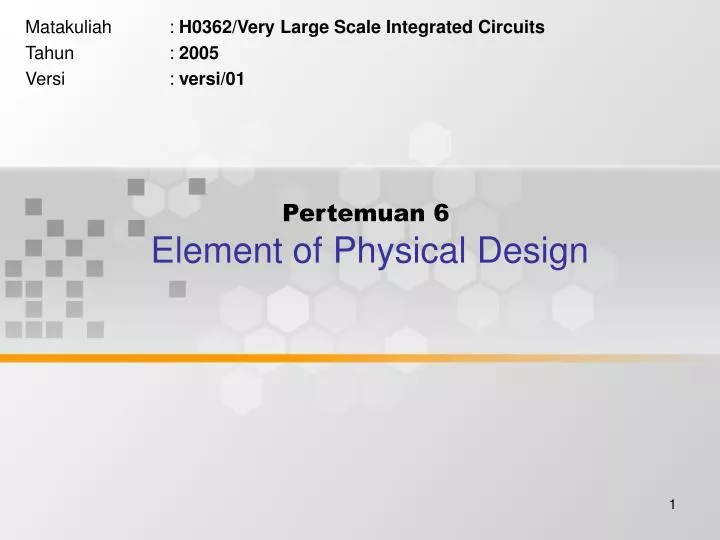
Pertemuan 6 Element of Physical Design. Matakuliah : H0362/Very Large Scale Integrated Circuits Tahun : 2005 Versi : versi/01. Learning Outcomes. Pada Akhir pertemuan ini, diharapkan mahasiswa akan dapat menyebutkan element-element dalam physiscal design proses VLSI.

E N D
Pertemuan 6Element of Physical Design Matakuliah : H0362/Very Large Scale Integrated Circuits Tahun : 2005 Versi : versi/01
Learning Outcomes Pada Akhir pertemuan ini, diharapkan mahasiswa akan dapat menyebutkan element-element dalam physiscal design proses VLSI.
Physical design is the actual process of creating circuits on silicon. Polygon in physical design Basic Concepts
Layout of Basic Structure Masking sequence • Start with p-type substrate • nWell • Active • Poly • pSelect • nSelect • Active contact • Poly contact • Metal 1 • Via • 10. Metal 2 • 11. Overglass
n-well Snw-nw n-well n-well p-substrate Cross-section Wnw Wnw Mask set FOX Active Active Active Sa-a Wa Silicon substrate Active pattern Cross-section Layout of Basic Structure
nSelect nSelect Active n+ regions: Sa-n FOX FOX Wa n+ Sa-n p Active Cross-section Mask set p+ regions: nSelect Sp-nw nSelect Active Sa-n Wa FOX p+ Sa-n FOX n-well Sp-nw Active Mask set Cross-section Layout of Basic Structure
Active poly nSelect nFET: L poly W n+ n+l p dpo Cross-section Mask set Active poly pFET: pSelect n-well L poly W p+ p+l n-well dpo p Cross-section Mask set Layout of Basic Structure
Active select Active contact Active contact dac, v Sa-ac p+ n+ n-well p dac, h Cross-section Generl mask set select Sm1-ac Metal 1 Wm1 Ox n+ p Metal 1 Active Cross-section Generl mask set Layout of Basic Structure
VDD Logic gate as basic cells VDD VDD VDD in VDD XNOR2 XNOT VDD XNAND2 out in1 in1 out out VSS VSS in2 in2 VSS VSS VSS VSS 2 XNOT + XNAND2 VDD VDD a a f f b b VSS VSS New complex cells Primitive cells Cell Concepts
VDD nWell pFET Pm1-m1 Dm1-m1 nFET p-substrate VSS VDD nWell horizontal vertical VSS Cell Concepts
VDD VDD D1 nWell nWell D2 VSS VSS X2 X1 Vertical FET Horizontal FET 2 4 1 3 4 1 3 2 Larger Smaller Cell Concepts
Vertical metal 2 VDD Logic cells VSS Metal 1 wiring VDD Logic cells VSS Metal 1 wiring VDD Logic cells VSS Cell Concepts
VDD Logic cells VSS Inverted Logic cells VDD Logic cells VSS Inverted Logic cells VDD Metal 2 Weinberger image array nWell VDD pFET VDD pFET nWell Metal input Logic row p-substrate Metal output nFET VSS VSS p-substrate nFET Logic row To wiring channel pFET nWell VDD Port placement in a cel FET placement in Weinberger array Cell Concepts
VDD X X X Mp NOT GATE X nWell VDD X Mp Mn X Gnd Mn Physical Design Logic Gate
RESUME • Basic Concepts. • Layout of Basic Structure. • Cell Concepts. • Physical Design Logic Gate.