Download
1 / 13
130 likes | 143 Views
Explore the optimization of ABCN Front-End for short strips and the evolution of shunt regulation options. Details on clock/data rates, power budgets, and regulation schemas presented in July 2007. Consider adaptation to various power scenarios.

E N D
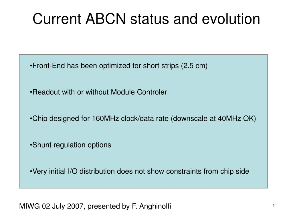
Current ABCN status and evolution • Front-End has been optimized for short strips (2.5 cm) • Readout with or without Module Controler • Chip designed for 160MHz clock/data rate (downscale at 40MHz OK) • Shunt regulation options • Very initial I/O distribution does not show constraints from chip side MIWG 02 July 2007, presented by F. Anghinolfi
Power Budget Update Front-End has been optimized for short strips (2.5 cm) Estimate Analogue current : 33 mA (@ 2.3V regulated voltage, 2.5V voltage source) Estimate of digital current : 92mA (@ 2.5V) 2
Readout Schema Slide 1 Readout with MC 160MHz generated from MC Each ABCN receives 160MHz Clock and CMD lines (driven by MC) The CMD line transmits Cmd bits and a sync signal to generate internal 40MHz BC rate ABCN ABCN S S MC Tok Data Tok Data Tok Data Tok Data Tok Data Data Out data 160MhZ Base CLK CMDin Local CLK CMDin Base CLK CMDin Base CLK CMDin CMD 160MHz mode 160MHz mode
Readout Schema Slide 1 Standalone Each ABCN receives 160MHz Clock and CMD lines The CMD line transmits Cmd bits and a sync signal to generate internal 40MHz BC rate ABCN ABCN ABCN Out Tok/Data Out Tok/Data Out Tok/Data In Tok/Data In Tok/Data In Tok/Data M S S 160MhZ Base CLK CMDin Base CLK CMDin Base CLK CMDin CMD 160MHz mode 160MHz mode 160MHz mode data
160MHZ Clock/CMD system Each ABCN receives 160MHz Clock and CMD lines The CMD line transmits Cmd bits and a sync signal to generate internal 40MHz BC rate. Possibility to transmit both Command and L1 signals 160MHz clock CMD sync Preliminary L1 Command bit 40MHz internal clock Idea/Schema developed by Mitch/Penn U.
Regulation Schema The Shunt concept is evolving from a shunt device per ABCN, and one common control (feedback) element in the module controler to : One shunt regulator per ABCN (as in the original proposal) but with some feature to distribute shunt currents through all ABCN circuits in parallel
Actual presentation of powering schema with ABCN I input ABCN 2.8V 2.5V LDVR Shunt regulator (external) 2.8V 2.5V LDVR I output External decoupling 100nF (200nF) • Some drawbacks • - additional power dissipation • ABCN_digital needs 2.5 V • ABCN_analog can work with 2.2 V • single point with high power dissipation on the hybrid • The option with a shunt regulator on the ABCN is investigated further
On-chip shunt regulator • We need good quality of digital power supply – requires a ”strong” shunt regulator with high gain and low output resistance • Parallel connection of shunt regulators becomes very sensitive to matching of parameters • N.B. This idea against the fundamental rules of electrical engineering and circuit theory • Intermediate solution (proposed by M. Weber) – external regulator per module and individual shunt transistors in each ABCN connected in parallel • avoids sensitivity to matching of reference voltages (band-gap reference) • still sensitive to matching of shunt transistors • in addition shunt regulator structure includes hybrid parasitic components in the feedback loop – more difficult to design for stability
On-chip shunt regulators in parallel • 10 ABCNs in parallel • Assumed current draws • digital: 10 mA without clock, 110 mA with clock • analog: 20 mA after power-up, 30 mA nominal operation • Total current delivered from an external source 1.6 A
On-chip shunt regulators in parallel Basic principle works but requires more studies of various scenario Clock ON At power-up and in nominal operation all shunt curent taken by one shunt regulator
New development Basic principle works but it requires more studies and better understanding of various power scenarios Trigger ON Clock ON Fine reference adjustment when ABCN active Self-adjustment of the reference at power-up – sets a maximum current for each shunt transistor and forces more uniform distribution of current
Chip size & Bonding Number of pads frontend pads zone 7.5 mm 5-7 mm