Download
1 / 22
230 likes | 429 Views
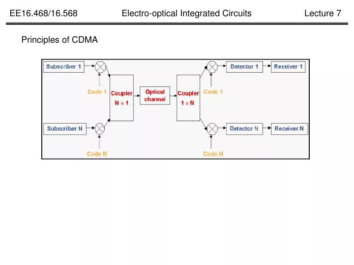
Principles of CDMA. Optical CDMA advantages:. Perform signal encoding/decoding in optical domain directly – potentially high speed (>100Gbit/s). Avoid electrical/optical and optical/electrical conversion bottleneck. Efficient bandwidth utilization.

E N D
Optical CDMA advantages: • Perform signal encoding/decoding in optical domain directly – potentially high speed (>100Gbit/s). • Avoid electrical/optical and optical/electrical conversion bottleneck. • Efficient bandwidth utilization. • Data format and protocol transparent – simplified architecture and network maintenance. • Simplified network architecture, less equipment inventory, flexible, scalable network.
Challenges: • Accurate and tunable phase control • All-optical switch and amplitude modulation • Integrated circuits with these functionalities Polymeric waveguide based photonic circuits: • Large electro-optic (EO) and Thermo-Optic coefficients: • - polymer TO ~ -1.4 x 10⁻⁴/°C; silica, T.O. ~ 1 x 10⁻⁵/°C • - Polymer EO ~ 80pm/V, LiNbO3 ~ 33pm/V • Low dielectric constant -- Potentially high–speed operation: • - polymer: r ~ 2.3, Si: r ~ 10 • - Capacitance ~ 5 times smaller than Si based circuits.
4 Electro-optic SSB modulator Si Electronics l1, l2, l3 l filter EO phase shifter Amplifier Polymeric waveguide based photonic circuits: • Multifunction capability --- Photonic integrated circuits • Flexible substrate, low cost and relative simple fabrications
Received signal SNR • High bit error rate (BER) due to correction noise. • Need long sequence to reduce the correction error.
Optical CDMA Modulation CDMA modulated signal CDMA modulated signal Channel 1 Channel 1 Channel 2 Channel 2
Received signal Time scale 25ps/100units CDMA demodulated channel 1 signal CDMA demodulated channel 2 signal
100Gb/s Tranceivers Difficulties of traditional transceivers • High-speed (>40Gb/s) external modulators not available. • Extremely difficult to achieve CDR using high-bandwidth (>40GHz) electronic circuitry even with low k and scale VLSI technologies. • SNR degradation for ultra-high frequency circuitry. • Very expensive.
100Gb/s All-optical Transceiver Interface Module Why All-optical Module • Interface the relative slow electronics circuit. • Perform pulse reshape and retiming without OE-EO conversion. • Future all-optical packet routing. Challenges: • 100GHz optical clock generation. • Optical threshold gate. • Re-shaping and re-timing.
Architecture of 100Gb/s Transceiver Interface Module • Photonics integrated circuit approach • Precisely controlled time delays
Architecture of 100Gb/s Transceiver Module Pulse compressor:
Kerr Nonlinearity in Semiconductors Kerr Nonlinearity: in InP semiconductor • Index change and tuning range: • For high index contrast (3.5:1), 10mW laser power induces index changes of 0.03. • Pulse compression ratio >10.
Architecture of 100Gb/s Transceiver Module Re-timing and re-shaping: