Download

1 / 64
640 likes | 651 Views
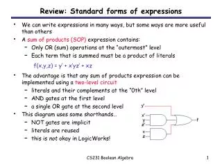
Standard Forms. Some Terms. Product: The Logical AND, not Arithmetic Multiply Operation Sum: The Logical OR , not Arithmetic Add Operation Canonical Form ( 正規形式 ) Min-terms ( 全及項 的和 ) Max-terms ( 全或項的積 ) Standard Form ( 一般形式 ) SOP - Sum of Products ( 積項和 ) POS - Product of Sums ( 和項積 ).

E N D
Standard Forms NTU DSD (Digital System Design) 2007
Some Terms • Product: The Logical AND, not Arithmetic Multiply Operation • Sum: The Logical OR , not Arithmetic Add Operation • Canonical Form (正規形式) • Min-terms (全及項的和) • Max-terms (全或項的積) • Standard Form (一般形式) • SOP - Sum of Products (積項和) • POS - Product of Sums (和項積) Jackie Kan - 2007 (jackiekan@LinTon.1D24H.com/jackiekan@csie.ntu.edu.tw) http://linton.1d24h.com/~jackiekan/
Min-term (全及項的和) Canonical Form (正規形式) • A product term (AND Term) in which all the variables appear exactly once, either complemented or uncomplemented, is called min-term. • There are 2n distinct min-terms for n variables. Jackie Kan - 2007 (jackiekan@LinTon.1D24H.com/jackiekan@csie.ntu.edu.tw) http://linton.1d24h.com/~jackiekan/
Maxterm (全或項的積) Canonical Form (正規形式) • A sum term (OR Term) that contains all the variables in complemented or uncomplemented form is called a max-term. • There are 2n distinct max-terms for n variables. Jackie Kan - 2007 (jackiekan@LinTon.1D24H.com/jackiekan@csie.ntu.edu.tw) http://linton.1d24h.com/~jackiekan/
DeMorgan’s Laws • DeMorgan’s Laws provide an easy way to find the inverse of a Boolean expression: • (X + Y)’ = X’ Y’ • (XY)’ = X’ + Y’ • An easy way to remember this is that each TERM is complemented, and that ORs become ANDs; ANDs become ORs. • Easy to prove this via a truth table Jackie Kan - 2007 (jackiekan@LinTon.1D24H.com/jackiekan@csie.ntu.edu.tw) http://linton.1d24h.com/~jackiekan/
Sum of Products (SOP/積項和) Expression • A sum of products expression is formed as follows. • Each row of the truth table in which the function takes on the value 1 contributes an ANDed term, using the asserted variable if there is a 1 in its column for that row or its complement if there is a 0. These are called min-terms. • A min-term is defined as an ANDed product of literals in which each variable appears exactly once in either true or complemented form, but not both. • The min-terms are then ORed to form the expression for the function. The min-term expansion is unique because it is deterministically derived from the truth table. Jackie Kan - 2007 (jackiekan@LinTon.1D24H.com/jackiekan@csie.ntu.edu.tw) http://linton.1d24h.com/~jackiekan/
Sum of Products (SOP/積項和) Normal Form (一般形式) • A Boolean expression is in Sum Of Products form when all products are the products of single variables only • F = AB’ + CD’E + AC’E’ SOP Form • G = ABC’ + DEFG + H SOP Form • H = AA’ + ABC + ABC’ Not SOP Form, Non-Standard Form • Y = A + B’ + C + D SOP Form • Z = (A+B)CD + EF Not SOP Form, Non-Standard Form = ACD + BCD + EF SOP Form Jackie Kan - 2007 (jackiekan@LinTon.1D24H.com/jackiekan@csie.ntu.edu.tw) http://linton.1d24h.com/~jackiekan/
Product of Sums (POS/和項積) Expression • A product of sums expression is formed as follows. • Each row of the truth table in which the function takes on the value 0 contributes an ORed term, using the complemented variable if there is a 0 in its column for that row or its complement if there is a 1. These are called max-terms. • A max-term is defined as an ORed product of literals in which each variable appears exactly once in either true or complemented form, but not both. • The max-terms are then ANDed to form the expression for the function. The max-term expansion is unique because it is deterministically derived from the truth table. Jackie Kan - 2007 (jackiekan@LinTon.1D24H.com/jackiekan@csie.ntu.edu.tw) http://linton.1d24h.com/~jackiekan/
Product of Sums (POS/和項積) Normal Form (一般形式) • A Boolean expression is in Product Of Sums form when all sums are the sums of single variables • F = (A + B’)(C + D’ + E)(A + C’ + E’) POS Form • G = A (B + E)(C + D) POS Form • Y = AB + AC Not POS Form, SOP Form = (A)(B + C) POS Form Jackie Kan - 2007 (jackiekan@LinTon.1D24H.com/jackiekan@csie.ntu.edu.tw) http://linton.1d24h.com/~jackiekan/
Decimal Notation • Sum of Min-terms • F(A,B,C) = Σm(0, 4, 5)= m0 + m4 + m5= A'B'C' + AB'C' + AB'C • Product of Max-terms • F(A,B,C) = ΠM(1,2,3,6,7)= (M1)(M2)(M3)(M6)(M7)= (A+B+C')(A'+B+C')(A+B’+C’)(A’+B’+C)(A’+B’+C’) • For an n Variables Function • Number of Min-terms + Number of Max-terms = 2n (2的n次方個) Jackie Kan - 2007 (jackiekan@LinTon.1D24H.com/jackiekan@csie.ntu.edu.tw) http://linton.1d24h.com/~jackiekan/
SOP Canonical/Standard and Minimal Form • F in CSOP canonical (SOP標準式/Standard) form : F(A, B, C) = ∑m(1,3,5,6,7) = m1 + m3 + m5 + m6 + m7 • = A'B'C + A'BC + AB'C + ABC' + ABC • canonical form (正規式) minimal form (最簡式) • F(A, B, C) = A'B'C + A'BC + AB'C + ABC + ABC' • = (A'B' + A'B + AB' + AB)C + ABC' • = ((A' + A)(B' + B))C + ABC'= C + ABC'= ABC' + C • = AB + C (最簡式) Jackie Kan - 2007 (jackiekan@LinTon.1D24H.com/jackiekan@csie.ntu.edu.tw) http://linton.1d24h.com/~jackiekan/
POS Canonical/Standard and Minimal Form • F in CPOS canonical (POS標準式/Standard) Form: F(A, B, C) = ΠM(0,2,4) = M0 • M2 • M4 • = (A+B+C) (A+B'+C) (A'+B+C) • canonical form (正規式) minimal form (最簡式) • F(A, B, C) = (A+B+C) (A+B'+C) (A'+B+C) • = (A + B + C) (A + B' + C) • (A + B + C) (A' + B + C) • = (A + C) (B + C) (最簡式) Jackie Kan - 2007 (jackiekan@LinTon.1D24H.com/jackiekan@csie.ntu.edu.tw) http://linton.1d24h.com/~jackiekan/
Summary • Sum of Products (SOP): AND-of-Ors / Product of Sums (POS): OR-of-ANDs • Canonical Sum of Products / Product of Sums (CSOP/CPOS) 正規式 • Any Boolean function that is expressed as a sum of min-terms, or as a product of max-terms is said to be in its canonical form. • F = x' y z + x y' z + x y z' + x y z • F' = (x+y'+z') • (x'+y+z') • (x'+y'+z) • (x'+y'+z') • Normal Sum of Products/Product of Sums (NSOP/NSOP) 一般式 • A Boolean function is said to be in a normal form if a sum-of-products expression or a product-of-sums expression has at least one term that is not a min-term or a max-terms respectively. • F = xy'z + xyz' + yz • Non-Standard Form or Non-Normal Form非一般式 • common variables in a normal form expression can be factored out. The resulting expression is no longer in a sum-of-products or product-of-sums format. These expressions are in a non-standard form or non-normal form. • F = x(y'z + yz') + yz • Minimal Form 最簡式 • Need simplified the expression Jackie Kan - 2007 (jackiekan@LinTon.1D24H.com/jackiekan@csie.ntu.edu.tw) http://linton.1d24h.com/~jackiekan/
Quiz 1 • Please complete the follows table Jackie Kan - 2007 (jackiekan@LinTon.1D24H.com/jackiekan@csie.ntu.edu.tw) http://linton.1d24h.com/~jackiekan/
NAND & NOR Gates NTU DSD (Digital System Design) 2007
NAND, NOR Gates • Why do we care about DeMorgan’s Law? • There are two other gate types that produce thecomplement of a boolean function! A B Y A B Y 0 0 1 0 0 1 0 1 1 0 1 0 1 0 1 1 0 0 1 1 0 1 1 0 A A Y=(AB)’ Y=(A+B)’ B B Jackie Kan - 2007 (jackiekan@LinTon.1D24H.com/jackiekan@csie.ntu.edu.tw) http://linton.1d24h.com/~jackiekan/
NAND, NOR • NAND (NOT AND) • Can be thought of as an AND gate followed by an inverter • NOR (NOT OR) • Can be thought as an OR gate followed by an inverter A Y=(AB)’ A Y=(AB)’ AB B B A Y=(A+B)’ A Y=(A+B)’ A+B B B Jackie Kan - 2007 (jackiekan@LinTon.1D24H.com/jackiekan@csie.ntu.edu.tw) http://linton.1d24h.com/~jackiekan/
Actually …. • In the real world • An AND gate is made from a NAND gate followed by an inverter • An OR gate is made from a NOR gate followed by an inverter Jackie Kan - 2007 (jackiekan@LinTon.1D24H.com/jackiekan@csie.ntu.edu.tw) http://linton.1d24h.com/~jackiekan/
G G S D S D N-channelopen when voltage at G is lowcloses when: voltage(G) > voltage (S) + P-channelclosed when voltage at G is lowopens when: voltage(G) < voltage (S) – MOS Transistor • MOS transistors have three terminals: drain, gate, and source • They act as switchesas follows: • if voltage on gate terminal is (some amount) higher/lower than source terminal then a conducting path is established between drain and source terminals Jackie Kan - 2007 (jackiekan@LinTon.1D24H.com/jackiekan@csie.ntu.edu.tw) http://linton.1d24h.com/~jackiekan/
G N-MOS G = 0, S-D Off / G = 1, On S D G P-MOS G = 0, S-D On / G = 1, Off S D MOS Network • X 與 Y 的關係為何 Jackie Kan - 2007 (jackiekan@LinTon.1D24H.com/jackiekan@csie.ntu.edu.tw) http://linton.1d24h.com/~jackiekan/
G N-MOS G = 0, S-D Off / G = 1, On S D G P-MOS G = 0, S-D On / G = 1, Off S D Using CMOS Implement AND Gate Jackie Kan - 2007 (jackiekan@LinTon.1D24H.com/jackiekan@csie.ntu.edu.tw) http://linton.1d24h.com/~jackiekan/
G N-MOS G = 0, S-D Off / G = 1, On S D G P-MOS G = 0, S-D On / G = 1, Off S D Using CMOS Implement OR Gate Jackie Kan - 2007 (jackiekan@LinTon.1D24H.com/jackiekan@csie.ntu.edu.tw) http://linton.1d24h.com/~jackiekan/
S1 S2 S2 S1 S4 S3 S4 S3 Using CMOS Implement NAND / NOR Gate Jackie Kan - 2007 (jackiekan@LinTon.1D24H.com/jackiekan@csie.ntu.edu.tw) http://linton.1d24h.com/~jackiekan/
S2 S1 S4 S3 CMOS – AND 與 NAND • Propogation Delay 傳輸延遲 • AND - 2, NAND - 1 • MOS電晶體數 • AND – 6個, NAND – 4個 Jackie Kan - 2007 (jackiekan@LinTon.1D24H.com/jackiekan@csie.ntu.edu.tw) http://linton.1d24h.com/~jackiekan/
S1 S2 S3 S4 CMOS – OR 與 NOR • Propogation Delay 傳輸延遲 • OR - 2, NOR - 1 • MOS電晶體數 • OR – 6個, NOR – 4個 Jackie Kan - 2007 (jackiekan@LinTon.1D24H.com/jackiekan@csie.ntu.edu.tw) http://linton.1d24h.com/~jackiekan/
NAND-NAND Form = AND-OR Form A (AB)’ F = ((AB)’ (CD)’)’ B C (CD)’ D SameLogicFunction A AB F = AB+CD B C CD D Jackie Kan - 2007 (jackiekan@LinTon.1D24H.com/jackiekan@csie.ntu.edu.tw) http://linton.1d24h.com/~jackiekan/
NOR-NOR Form = OR-AND Form A (A+B)’ F = ((A+B)’ (C+D)’)’ B C (C+D)’ D SameLogicFunction A A+B F = (A+B)(C+D) B C C+D D Jackie Kan - 2007 (jackiekan@LinTon.1D24H.com/jackiekan@csie.ntu.edu.tw) http://linton.1d24h.com/~jackiekan/
Summary Jackie Kan - 2007 (jackiekan@LinTon.1D24H.com/jackiekan@csie.ntu.edu.tw) http://linton.1d24h.com/~jackiekan/
Summary Jackie Kan - 2007 (jackiekan@LinTon.1D24H.com/jackiekan@csie.ntu.edu.tw) http://linton.1d24h.com/~jackiekan/
SOP and POS Examples jackiekan@solutioninside.com NTU DSD (Digital System Design) 2007
SOP & POS F = ∑m(1,3,5,7) = A’B’C+A’BC+AB’C+ABC F’ = ΠM(0,2,4,6) = (A+B+C)(A+B’+C) (A’+B+C)(A’+B’+C) F’ = ∑m(0,2,4,6) = A’B’C’+A’BC’+AB’C’+ABC’ F = (A’B’C’+A’BC’+AB’C’+ABC’)’ = (A’B’C’)’(A’BC’)’(AB’C’)’(ABC’)’ = (A+B+C)(A+B’+C) (A’+B+C)(A’+B’+C) Jackie Kan - 2007 (jackiekan@LinTon.1D24H.com/jackiekan@csie.ntu.edu.tw) http://linton.1d24h.com/~jackiekan/
Simulation Program (Verilog Code) • F(A,B,C,D) = ∑m(3,4,5,6,7,11,14) module myf1(f,a,b,c,d); output f; input a,b,c,d; //MAX (0,1,2,8,9,10,12,13,15) assign f = ((a|b|c|d) & (a|b|c|!d) & (a|b|!c|d) & (!a|b|c|d) & (!a|b|c|!d) & (!a|b|!c|d) & (!a|!b|c|d)& (!a|!b|c|!d) & (!a|!b|!c|!d)); endmodule module myf2(f,a,b,c,d); output f; input a,b,c,d; //MIN (3,4,5,6,7,11,14) assign f = ((!a&!b&c&d) | (!a&b&!c&!d) | (!a&b&!c&d) | (!a&b&c&!d) | (!a&b&c&d) | (a&!b&c&d) | (a&b&c&!d) ); endmodule Jackie Kan - 2007 (jackiekan@LinTon.1D24H.com/jackiekan@csie.ntu.edu.tw) http://linton.1d24h.com/~jackiekan/
Simulation Results 0 1 2 3 4 5 6 7 8 9 10 11 12 13 14 15 f1=MAX(0,1,2,8,9,10,12,13,15) f2=MIN (3,4,5,6,7,11,14) Jackie Kan - 2007 (jackiekan@LinTon.1D24H.com/jackiekan@csie.ntu.edu.tw) http://linton.1d24h.com/~jackiekan/
Quiz 2) Please draw the AND-OR form and OR-AND form circuits of F1 & F2. F1 = MIN (3, 5, 6, 7, 11) F2’ = Σm (2, 7, 13, 14, 15) 3) Draw the Truth Table, Minterm and Maxterm, and ALL-NAND Circuit of F3 & ALL-NOR Circuit of F4. F3 = A’BC+AB’CD’+ABC’+A’B’CD F4’ = AB + CB + D’E Note: All gates must be only 2-inputs and 1-output in Quiz 3. Jackie Kan - 2007 (jackiekan@LinTon.1D24H.com/jackiekan@csie.ntu.edu.tw) http://linton.1d24h.com/~jackiekan/
Enable and Inhibit Properties of Logic Gates NTU DSD (Digital System Design) 2007
AND Gate A Y B A B Y Gate Inhibited Gate Enabled Jackie Kan - 2007 (jackiekan@LinTon.1D24H.com/jackiekan@csie.ntu.edu.tw) http://linton.1d24h.com/~jackiekan/
OR Gate A Y B A B Y Gate Enabled Gate Inhibited Jackie Kan - 2007 (jackiekan@LinTon.1D24H.com/jackiekan@csie.ntu.edu.tw) http://linton.1d24h.com/~jackiekan/
NAND Gate A Y B A B Y Gate Inhibited Gate Enabled Jackie Kan - 2007 (jackiekan@LinTon.1D24H.com/jackiekan@csie.ntu.edu.tw) http://linton.1d24h.com/~jackiekan/
NOR Gate A Y B A B Y Gate Enabled Gate Inhibited Jackie Kan - 2007 (jackiekan@LinTon.1D24H.com/jackiekan@csie.ntu.edu.tw) http://linton.1d24h.com/~jackiekan/
XOR Gate A Y B A B Y Gate Enabled Gate Inhibited (True) (Complement) Jackie Kan - 2007 (jackiekan@LinTon.1D24H.com/jackiekan@csie.ntu.edu.tw) http://linton.1d24h.com/~jackiekan/
Summary of Enable/Inhibit Properties Control AND OR NAND NOR XOR XNOR A=0 Y=0 Y=B Y=1 Y=B’ Y=B Y=B’ A=1 Y=B Y=1 Y=B’ Y=0 Y=B’ Y=B Jackie Kan - 2007 (jackiekan@LinTon.1D24H.com/jackiekan@csie.ntu.edu.tw) http://linton.1d24h.com/~jackiekan/
IC Family NTU DSD (Digital System Design) 2007
Family Characteristics • TTL • Transistor-based • Faster than CMOS • Larger current carrying capability • Higher power consumption • High voltage requirements • CMOS • MOSFET-based • Greater noise immunity • Low power consumption • Variable voltage requirements • Low speed Jackie Kan - 2007 (jackiekan@LinTon.1D24H.com/jackiekan@csie.ntu.edu.tw) http://linton.1d24h.com/~jackiekan/
Transistor ON & OFF • 飽和區(ON) • 截止區(OFF) B-E沒有偏壓或逆向偏壓 B-E順向偏壓且有足夠大的IB Jackie Kan - 2007 (jackiekan@LinTon.1D24H.com/jackiekan@csie.ntu.edu.tw) http://linton.1d24h.com/~jackiekan/
TTL IC Characteristics • 基本電路(ex. NOT Gate) = 輸入層 驅動層 輸出層 Jackie Kan - 2007 (jackiekan@LinTon.1D24H.com/jackiekan@csie.ntu.edu.tw) http://linton.1d24h.com/~jackiekan/
TTL IC Characteristics • 當輸入為HI,則輸出為LO • 當輸入為LO,則輸出為HI Jackie Kan - 2007 (jackiekan@LinTon.1D24H.com/jackiekan@csie.ntu.edu.tw) http://linton.1d24h.com/~jackiekan/
A B ICQ1 Q1 Q2 Q3 Q4 Y O/P 0 0 + ON OFF OFF ON 1 0 1 + ON OFF OFF ON 1 1 0 + ON OFF OFF ON 1 1 1 - OFF ON ON OFF 0 TTL NAND Jackie Kan - 2007 (jackiekan@LinTon.1D24H.com/jackiekan@csie.ntu.edu.tw) http://linton.1d24h.com/~jackiekan/
Propagation Delay • Delay Definitions Jackie Kan - 2007 (jackiekan@LinTon.1D24H.com/jackiekan@csie.ntu.edu.tw) http://linton.1d24h.com/~jackiekan/
Propagation Delay TTL measured at 1.5Volt mark CMOS measured at 50% mark Jackie Kan - 2007 (jackiekan@LinTon.1D24H.com/jackiekan@csie.ntu.edu.tw) http://linton.1d24h.com/~jackiekan/
Propagation Delay • Propagation Delay in a circuit is the sum of all the propagation delays in the output path • Always use the worst-case when designing. Jackie Kan - 2007 (jackiekan@LinTon.1D24H.com/jackiekan@csie.ntu.edu.tw) http://linton.1d24h.com/~jackiekan/