Download
1 / 13
130 likes | 419 Views
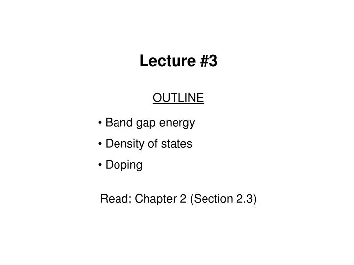
Lecture #3. OUTLINE Band gap energy Density of states Doping Read: Chapter 2 (Section 2.3). Band Gap and Material Classification. E. c. = . E. ~9 eV. G. E. c. =. E. 1.12 eV. G. E. E. E. v. v. c. metal. SiO 2. Si.

E N D
Lecture #3 OUTLINE Band gap energy Density of states Doping Read: Chapter 2 (Section 2.3)
Band Gap and Material Classification E c = E ~9 eV G E c = E 1.12 eV G E E E v v c metal SiO2 Si • Filled bands and empty bands do not allow current flow • Insulators have large EG • Semiconductors have small EG • Metals have no band gap • conduction band is partially filled EE130 Lecture 3, Slide 2
electron E c photon photon energy: h v E G E v hole Measuring Band Gap Energy · EG can be determined from the minimum energy (hn) of photons that are absorbed by the semiconductor. Band gap energies of selected semiconductors EE130 Lecture 3, Slide 3
Density of States E gc(E) DE E E c c E E v v gv(E) g(E)dE = number of states per cm3 in the energy range between E and E+dE Near the band edges: E Ec EEv EE130 Lecture 3, Slide 4
Donors: P, As, Sb Acceptors: B, Al, Ga, In Doping By substituting a Si atom with a special impurity atom (Column V or Column III element), a conduction electron or hole is created. EE130 Lecture 3, Slide 5
Doping Silicon with Donors Example: Add arsenic (As) atom to the Si crystal The loosely bound 5th valence electron of the As atom “breaks free” and becomes a mobile electron for current conduction. EE130 Lecture 3, Slide 6
Doping Silicon with Acceptors Example: Add boron (B) atom to the Si crystal The B atom accepts an electron from a neighboring Si atom, resulting in a missing bonding electron, or “hole”. The hole is free to roam around the Si lattice, carrying current as a positive charge. EE130 Lecture 3, Slide 7
Donor / Acceptor Levels (Band Model) E c ED Donor Level Donor ionization energy Acceptor ionization energy Acceptor Level E A E v Ionization energy of selected donors and acceptors in silicon EE130 Lecture 3, Slide 8
Charge-Carrier Concentrations ND: ionized donor concentration (cm-3) NA: ionized acceptor concentration (cm-3) Charge neutrality condition: ND + p = NA + n At thermal equilibrium, np = ni2 (“Law of Mass Action”) Note: Carrier concentrations depend on net dopant concentration (ND - NA) ! EE130 Lecture 3, Slide 9
N-type Material ND >> NA (ND – NA >> ni): EE130 Lecture 3, Slide 10
P-type Material NA >> ND (NA – ND >> ni): EE130 Lecture 3, Slide 11
Terminology donor: impurity atom that increases n acceptor: impurity atom that increases p n-type material: contains more electrons than holes p-type material: contains more holes than electrons majority carrier: the most abundant carrier minority carrier: the least abundant carrier intrinsic semiconductor: n = p = ni extrinsic semiconductor: doped semiconductor EE130 Lecture 3, Slide 12
Summary • The band gap energy is the energy required to free an electron from a covalent bond. • EG for Si at 300K = 1.12eV • Insulators have large EG; semiconductors have small EG • Dopants in Si: • Reside on lattice sites (substituting for Si) • Group-V elements contribute conduction electrons, and are called donors • Group-III elements contribute holes, and are called acceptors • Very low ionization energies (<50 meV) ionized at room temperature Dopant concentrations typically range from 1014 cm-3 to 1020 cm-3 EE130 Lecture 3, Slide 13