Download
1 / 14
190 likes | 513 Views
Electric field control of Metal-insulator phase transition in VO2 nano-wire channel. Tsubasa Sasaki (Tanaka-lab). 2013/5/29. Contents. ・ Background Metal-insulator transition(MIT) of strongly-correlated electron(Mott) materials (ex. VO 2 ) How to control of MIT? Mott FET

E N D
Electric field control of Metal-insulator phasetransition in VO2 nano-wire channel Tsubasa Sasaki (Tanaka-lab) 2013/5/29
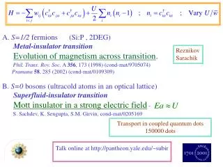
Contents ・Background Metal-insulator transition(MIT) of strongly-correlated electron(Mott) materials (ex. VO2) How to control of MIT? Mott FET ・Purpose of my research Control of MIT by electric field ・Principleof Mott transition ・My original model ・Experiment Pulsed laser deposition (PLD) Nano imprint lithography ・Result ・Summary
Background Temperature change strongly-correlated electron materials (強相関電子系材料) VO2 Mott insulator (モット絶縁体) Impurity doping Temperature Impurity doping Metal-insulator transition(MIT) Huge resistivity change (103~104Ω) (V3+,4+,W6+ )O2
Background How to control the MIT? Device VG Mott FET Gate Source Drain Metal Drain current Porpose of my reserch Control of MIT by electric field MIT : metal-insulator transition
Background Multiple Avalanche effect VO2 A. Sharoni et al, Phys. Rev. Lett. 101, 026404 (2008) M.M.Qazilbash et al, Science 318, 1750 (2007) Phase separation with 100 nm-sized domains around Metal-Insulator transition
Purpose Carrier doping by electric field Drain d Gate Using side-gate FET structures Control of MIT by carrier doping L W Insulator Gate Metal Source • Advantage • Doping only carrier(Not impurity doping) • Flexible(Electric field) • Observable(Domain) A VO2 Pt
Principle (Brinkman Rice) Effective mass changes greatly band filling is changed :Features of strongly-correlated electron system BR picture n0=1.69x1022 cm-3 not silicon Band filling: Carrier doping Effective mass changes dramatically
Principle (Mott transition) Mott criterion :Insulator :Mott transition :Metal VO2: [cm-3] Effective Bohr radius Insulator Metal [cm] P. P. Edwards et al, J. Phys. Chem,99 (1995) 5228
My original model Mott criterion(carrier doping) Carrier doping amount by electric field :Insulator :Mott transition :Metal [cm-3] In fact, since the experiment at finite temperature, it is necessary to consider the thermal excitation carrier. Carrier doping amount by thermal excitation [cm-3] Eg=0.12 eV kB=8.617 ev/K
My original model :Insulator :Mott transition :Metal Insulator Metal Metal Metal Electric field switching Insulator
Experiment(PLD) 基板 V2O5焼結体 Pulse laser deposition (PLD) Production of thin film ArF(λ=193nm) レーザ VO2 Al2O3 レーザ 基板
Experiment(nanoimprint) Production of structure optical micrograph A 0.5mm 4mm 4mm Process
Result VO2 AFM image Pt 400nm optical micrograph Nano wire 300nm A Successful production of side-gate FET structures
Summary I made an original model using temperature parameter (T) and gate voltage (Vg) combined with the BR picture and the Mott criterion ● I have successfully created side-gate FET structures ● Further work Electronic propaty measurement I will control MIT by electric field